
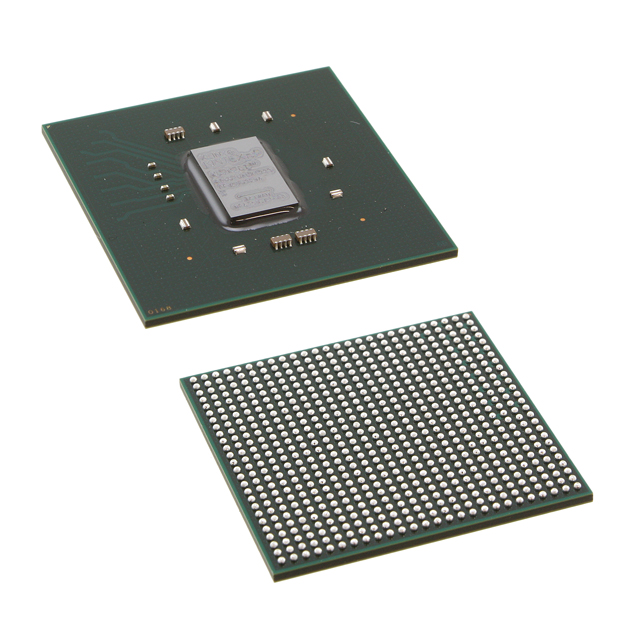
XC5VLX30-2FF676C
| Part Description |
Virtex®-5 LX Field Programmable Gate Array (FPGA) IC 400 1179648 30720 676-BBGA, FCBGA |
|---|---|
| Quantity | 1,344 Available (as of June 15, 2026) |

| Product Category | Field Programmable Gate Array (FPGA) |
|---|---|
| Manufacturer | AMD |
| Manufacturing Status | Active |
| Manufacturer Standard Lead Time | 12 Weeks |
| Datasheet |
Specifications & Environmental
| Device Package | 676-FCBGA (27x27) | Grade | Commercial | Operating Temperature | 0°C – 85°C | ||
|---|---|---|---|---|---|---|---|
| Package / Case | 676-BBGA, FCBGA | Number of I/O | 400 | Voltage | 950 mV - 1.05 V | ||
| Mounting Method | Surface Mount | RoHS Compliance | RoHS non-compliant | REACH Compliance | REACH Unaffected | ||
| Moisture Sensitivity Level | 4 (72 Hours) | Number of LABs/CLBs | 2400 | Number of Logic Elements/Cells | 30720 | ||
| Number of Gates | N/A | ECCN | 3A991D | HTS Code | 8542.39.0001 | ||
| Qualification | N/A | Total RAM Bits | 1179648 |
Overview of XC5VLX30-2FF676C – Virtex®-5 LX Field Programmable Gate Array (FPGA) IC, 400 I/O, 676-FCBGA
The XC5VLX30-2FF676C is a Virtex®-5 LX field programmable gate array (FPGA) IC offering a high density of programmable logic and on-chip memory in a 676-ball FCBGA package. It provides a combination of sizable logic resources, embedded RAM, and a large number of I/O for designs that require integrated, reprogrammable digital logic.
With 30,720 logic elements, approximately 1.18 Mbits of embedded memory and up to 400 I/O pins, this commercial-grade FPGA is suited to systems that need substantial on-chip resources while operating within standard commercial temperature and supply ranges.
Key Features
- Programmable Logic Capacity 30,720 logic elements for implementing complex, custom digital designs.
- Embedded Memory Approximately 1.18 Mbits of on-chip RAM to support buffering, state storage, and data processing without immediate dependency on external memory.
- I/O Density Up to 400 I/O pins to accommodate multiple parallel interfaces and external peripherals.
- Package & Mounting 676-FCBGA (27×27 mm) package case (676-BBGA, FCBGA) in a surface-mount form factor for high pin-count board designs.
- Power Core voltage supply range of 0.95 V to 1.05 V to match modern low-voltage systems.
- Operating Range & Grade Commercial grade with an operating temperature range of 0 °C to 85 °C.
- Environmental Compliance RoHS compliant.
Typical Applications
- High-density digital logic Implement large-scale, custom logic functions using 30,720 logic elements to consolidate multiple functions into a single device.
- I/O-intensive systems Support complex interface requirements and multiple peripheral connections with up to 400 I/O pins.
- On-chip buffering and state storage Use approximately 1.18 Mbits of embedded RAM for frame buffering, FIFOs, and local data storage to reduce external memory needs.
- Commercial electronic products Designed for commercial temperature environments (0 °C to 85 °C) and RoHS compliance for mainstream electronic products.
Unique Advantages
- Significant programmable capacity: 30,720 logic elements enable consolidation of complex logic and reduce the need for multiple discrete components.
- Substantial on-chip memory: Approximately 1.18 Mbits of embedded RAM can lower external memory dependencies and simplify board-level BOM.
- High I/O count: 400 I/O pins provide flexibility for parallel interfaces and diverse connectivity options without external multiplexing.
- Compact high-pin-count package: 676-FCBGA (27×27) delivers high density in a surface-mount package suitable for space-constrained PCBs.
- Low-voltage core operation: 0.95–1.05 V supply compatibility aligns with modern low-voltage digital systems.
- RoHS compliant: Supports environmental requirements for commercial products.
Why Choose XC5VLX30-2FF676C?
The XC5VLX30-2FF676C positions itself as a versatile commercial-grade FPGA with a balanced mix of logic, embedded memory and I/O resources. Its 30,720 logic elements and approximately 1.18 Mbits of on-chip RAM are well suited to consolidate complex digital functions while the 400 I/O pins enable broad system interfacing within a 676-FCBGA surface-mount package.
This device is appropriate for designers and procurement teams looking for a programmable, RoHS-compliant solution that operates in standard commercial temperature ranges and low-voltage core environments. It offers a straightforward platform for projects that require significant on-chip resources and high I/O density.
Request a quote or submit a pricing inquiry to evaluate XC5VLX30-2FF676C for your next design and to discuss availability and lead times.


Date Founded: 1969
Headquarters: Santa Clara, California, USA
Employees: 25,000+
Revenue: $22.68 Billion
Certifications and Memberships: ISO9001:2015, RoHS, REACH


