
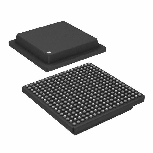
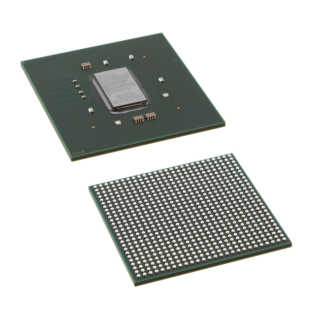
XC5VLX30-2FFG676C
| Part Description |
Virtex®-5 LX Field Programmable Gate Array (FPGA) IC 400 1179648 30720 676-BBGA, FCBGA |
|---|---|
| Quantity | 628 Available (as of June 10, 2026) |

| Product Category | Field Programmable Gate Array (FPGA) |
|---|---|
| Manufacturer | AMD |
| Manufacturing Status | Active |
| Manufacturer Standard Lead Time | 12 Weeks |
| Datasheet |
Specifications & Environmental
| Device Package | 676-FCBGA (27x27) | Grade | Commercial | Operating Temperature | 0°C – 85°C | ||
|---|---|---|---|---|---|---|---|
| Package / Case | 676-BBGA, FCBGA | Number of I/O | 400 | Voltage | 950 mV - 1.05 V | ||
| Mounting Method | Surface Mount | RoHS Compliance | ROHS3 Compliant | REACH Compliance | REACH Unaffected | ||
| Moisture Sensitivity Level | 4 (72 Hours) | Number of LABs/CLBs | 2400 | Number of Logic Elements/Cells | 30720 | ||
| Number of Gates | N/A | ECCN | 3A991D | HTS Code | 8542.39.0001 | ||
| Qualification | N/A | Total RAM Bits | 1179648 |
Overview of XC5VLX30-2FFG676C – Virtex®-5 LX Field Programmable Gate Array (FPGA), 676-FCBGA
The XC5VLX30-2FFG676C is a Virtex®-5 LX series FPGA from AMD, supplied in a 676-ball FCBGA package. It combines programmable logic, embedded memory, and a large count of user I/O to support configurable hardware designs in commercial applications.
With 2400 logic blocks (30720 logic elements), approximately 1.18 Mbits of on-chip RAM and up to 400 I/O pins, this device is suited to designs that require significant logic capacity, embedded memory and extensive external connectivity while operating within a commercial temperature range.
Key Features
- Core Logic 2400 logic blocks providing 30,720 logic elements for implementing custom digital circuitry and state machines.
- Embedded Memory Approximately 1.18 Mbits of on-chip RAM for packet buffers, FIFOs, small LUT-based storage and local data staging.
- I/O Capacity Up to 400 user I/O pins to support dense peripheral interfacing and multiple parallel interfaces.
- Power Core voltage supply range of 0.95 V to 1.05 V to match system power domains and regulator designs.
- Package & Mounting 676-ball FCBGA package (676-FCBGA, 27×27) in a surface-mount form factor for compact board implementations.
- Operating Conditions Commercial grade device rated for 0 °C to 85 °C operation and RoHS compliant for regulatory adherence in commercial products.
Typical Applications
- Embedded Systems Custom control and glue-logic implementations where programmable logic and on-chip memory enable tailored hardware functions.
- Prototyping & Development Hardware prototyping and design validation that benefit from reprogrammable logic capacity and flexible I/O.
- Communications & Interface Bridging Protocol adaptation and parallel interface aggregation using abundant I/O and embedded RAM for temporary buffering.
- Data Acquisition & Control I/O-dense control systems and data collection designs that require configurable logic and local memory resources.
Unique Advantages
- Substantial Logic Capacity: 30,720 logic elements deliver the resources needed for complex custom logic implementations.
- On-Chip Memory: Approximately 1.18 Mbits of embedded RAM reduces the need for external memory in many buffering and staging use cases.
- High I/O Count: 400 I/O pins provide flexibility for connecting multiple peripherals, buses and parallel signals without external expanders.
- Compact FCBGA Packaging: 676-ball FCBGA (27×27) enables a dense, surface-mount board layout for space-constrained designs.
- Commercial Temperature Rating: Rated for 0 °C to 85 °C operation and RoHS compliant to meet standard commercial product requirements.
- Defined Core Voltage Range: Core supply range of 0.95 V to 1.05 V facilitates integration with common voltage regulator solutions.
Why Choose XC5VLX30-2FFG676C?
The XC5VLX30-2FFG676C positions itself as a balanced, commercial-grade FPGA offering significant logic resources, embedded memory and a high I/O count in a compact FCBGA package. It is well suited for engineers and teams building configurable hardware that needs substantial on-chip resources and flexible interfacing.
For designs that require scalable programmable logic, local RAM and dense external connectivity while operating within commercial temperature limits, this Virtex-5 LX device provides a clear, specification-driven option backed by AMD’s FPGA product documentation.
Request a quote or submit a pricing inquiry to receive availability and purchasing information for the XC5VLX30-2FFG676C.


Date Founded: 1969
Headquarters: Santa Clara, California, USA
Employees: 25,000+
Revenue: $22.68 Billion
Certifications and Memberships: ISO9001:2015, RoHS, REACH


