
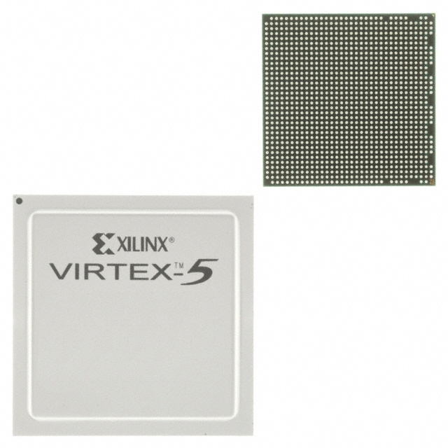
XC5VLX50-1FF676C
| Part Description |
Virtex®-5 LX Field Programmable Gate Array (FPGA) IC 440 1769472 46080 676-BBGA, FCBGA |
|---|---|
| Quantity | 246 Available (as of June 15, 2026) |

| Product Category | Field Programmable Gate Array (FPGA) |
|---|---|
| Manufacturer | AMD |
| Manufacturing Status | Active |
| Manufacturer Standard Lead Time | 12 Weeks |
| Datasheet |
Specifications & Environmental
| Device Package | 676-FCBGA (27x27) | Grade | Commercial | Operating Temperature | 0°C – 85°C | ||
|---|---|---|---|---|---|---|---|
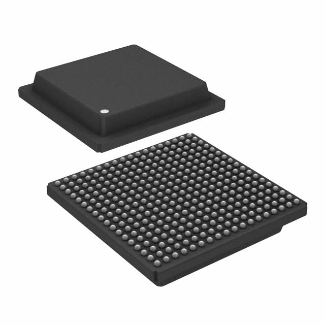
| Package / Case | 676-BBGA, FCBGA | Number of I/O | 440 | Voltage | 950 mV - 1.05 V | ||
| Mounting Method | Surface Mount | RoHS Compliance | RoHS non-compliant | REACH Compliance | REACH Unaffected | ||
| Moisture Sensitivity Level | 4 (72 Hours) | Number of LABs/CLBs | 3600 | Number of Logic Elements/Cells | 46080 | ||
| Number of Gates | N/A | ECCN | 3A991D | HTS Code | 8542.39.0001 | ||
| Qualification | N/A | Total RAM Bits | 1769472 |
Overview of XC5VLX50-1FF676C – Virtex®-5 LX FPGA, 676‑FCBGA
The XC5VLX50-1FF676C is a Virtex®-5 LX Field Programmable Gate Array (FPGA) IC offering substantial programmable logic, on-chip memory, and a high I/O count in a compact 676‑FCBGA package. It provides a configurable hardware platform for designers who require significant logic resources and embedded memory within a surface-mount, commercial-grade device.
Key device attributes include 46,080 logic elements, approximately 1.77 Mbits of on-chip RAM, 440 I/O, a 950 mV to 1.05 V supply range, and an operating temperature range of 0 °C to 85 °C.
Key Features
- Logic Resources 46,080 logic elements for implementing complex, high-density logic functions.
- Embedded Memory Approximately 1.77 Mbits of on-chip RAM (1,769,472 bits) to support data buffering, state storage, and local memory needs.
- I/O Capacity 440 available I/O pins to interface with external peripherals, memory, and system buses.
- Power and Core Voltage Core supply range from 950 mV to 1.05 V to match target system power architectures.
- Package Supplier device package: 676‑FCBGA (27 × 27), providing a high-pin-count flip-chip BGA form factor suitable for dense board designs.
- Mounting and Grade Surface-mount device, commercial grade with an operating temperature range of 0 °C to 85 °C.
- Regulatory RoHS compliant.
Unique Advantages
- High logic density: 46,080 logic elements enable implementation of large, complex digital designs without immediate need for external logic.
- Significant on-chip memory: Approximately 1.77 Mbits of embedded RAM reduces dependence on external memory for mid-sized data storage and buffering.
- Generous I/O availability: 440 I/O pins support extensive interfacing options for multi-peripheral systems.
- Compact, high-pin-count package: The 676‑FCBGA (27 × 27) package consolidates many signals in a space-efficient footprint for dense PCB layouts.
- Commercial temperature suitability: Rated 0 °C to 85 °C for a wide range of standard commercial applications.
- RoHS compliant: Meets common environmental compliance requirements for assembly.
Why Choose XC5VLX50-1FF676C?
The XC5VLX50-1FF676C positions itself as a high-capacity Virtex‑5 LX FPGA option that balances logic density, embedded memory, and extensive I/O in a single, surface-mount package. It is well suited for designers and procurement teams seeking a commercial-grade FPGA with measurable on-chip resources and a compact 676‑FCBGA footprint.
For projects that require a programmable, integrated logic platform with defined supply and temperature ranges, this part provides predictable electrical and mechanical characteristics to aid system integration and board-level planning.
Request a quote or submit a purchase inquiry to receive availability and pricing information for the XC5VLX50-1FF676C.


Date Founded: 1969
Headquarters: Santa Clara, California, USA
Employees: 25,000+
Revenue: $22.68 Billion
Certifications and Memberships: ISO9001:2015, RoHS, REACH


