
XC5VLX50-3FF676C
| Part Description |
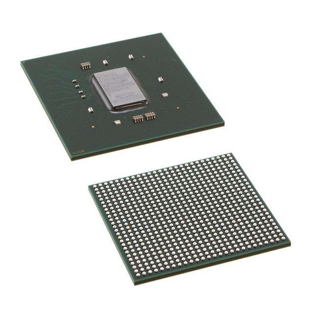
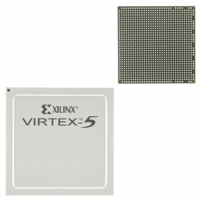
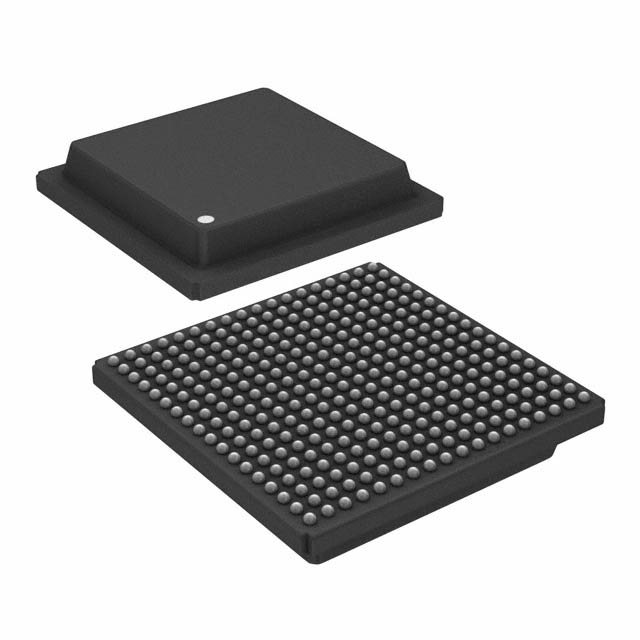
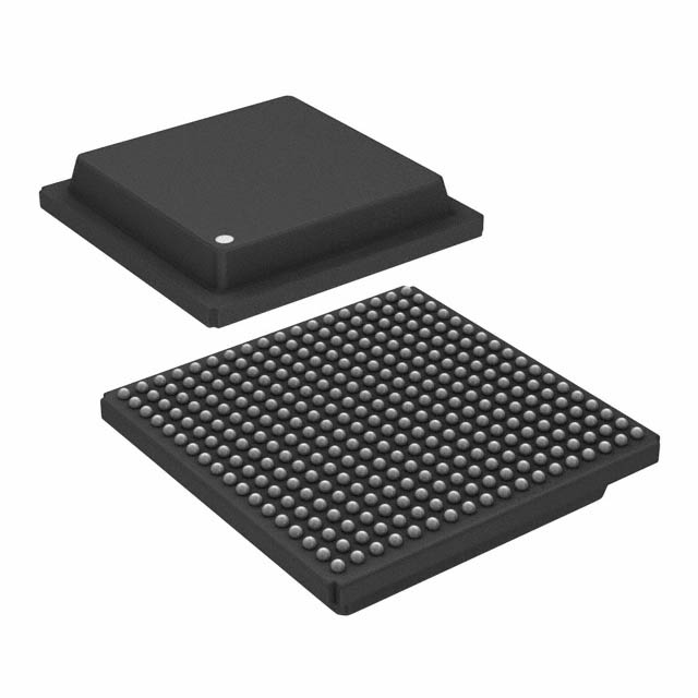
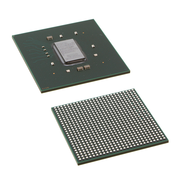
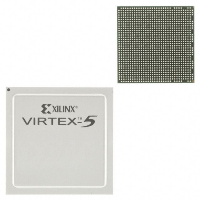
Virtex®-5 LX Field Programmable Gate Array (FPGA) IC 440 1769472 46080 676-BBGA, FCBGA |
|---|---|
| Quantity | 848 Available (as of October 8, 2026) |
| Product Category | Field Programmable Gate Array (FPGA) |
|---|---|
| Manufacturer | AMD |
| Manufacturing Status | Active |
| Manufacturer Standard Lead Time | 12 Weeks |
| Datasheet |
Specifications & Environmental
| Device Package | 676-FCBGA (27x27) | Grade | Commercial | Operating Temperature | 0°C – 85°C | ||
|---|---|---|---|---|---|---|---|
| Package / Case | 676-BBGA, FCBGA | Number of I/O | 440 | Voltage | 950 mV - 1.05 V | ||
| Mounting Method | Surface Mount | RoHS Compliance | RoHS non-compliant | REACH Compliance | REACH Unaffected | ||
| Moisture Sensitivity Level | 4 (72 Hours) | Number of LABs/CLBs | 3600 | Number of Logic Elements/Cells | 46080 | ||
| Number of Gates | N/A | ECCN | 3A991D | HTS Code | 8542.39.0001 | ||
| Qualification | N/A | Total RAM Bits | 1769472 |
Overview of XC5VLX50-3FF676C – Virtex®-5 LX Field Programmable Gate Array, 676‑FBGA
The XC5VLX50-3FF676C is a Virtex®-5 LX Field Programmable Gate Array (FPGA) in a 676-FCBGA package. It provides a dense programmable fabric with 3,600 CLBs and 46,080 logic elements, approximately 1.77 Mbits of embedded RAM and up to 440 user I/O in a 27 mm × 27 mm ball-grid array.
This commercial-grade FPGA targets designs that require high logic capacity, substantial on-chip memory and a large number of I/O signals while maintaining a compact surface-mount package and RoHS compliance.
Key Features
- Core Logic 3,600 CLBs delivering 46,080 logic elements for implementing complex custom logic and control functions.
- Embedded Memory Approximately 1.77 Mbits of on-chip RAM to support data buffering, state storage and localized memory structures.
- I/O Density Up to 440 user I/O pins, enabling high-density peripheral interfacing and board-level signal aggregation.
- Package & Mounting 676-FCBGA (27 × 27 mm) ball-grid array in a 676-BBGA format, designed for surface-mount assembly.
- Power Core voltage supply range from 950 mV to 1.05 V to match system power-rail requirements.
- Temperature & Grade Commercial grade with an operating temperature range of 0°C to 85°C.
- Regulatory RoHS compliant for lead-free manufacturing processes.
Typical Applications
- Custom logic implementations — Ideal for designs requiring tens of thousands of logic elements to implement control, glue logic or custom datapaths.
- Memory-dependent functions — Suited for applications that need approximately 1.77 Mbits of embedded RAM for buffering, lookup tables or local data storage.
- High-density I/O aggregation — Well suited for boards that require up to 440 programmable I/O for sensor arrays, interface bridging or multi-channel signaling.
- Compact board-level systems — The 676-FCBGA (27×27) surface-mount package supports compact, densely routed PCBs where package footprint and I/O count matter.
Unique Advantages
- Significant logic capacity: 46,080 logic elements enable implementation of sizable custom circuits without external gate arrays.
- Substantial on-chip memory: Approximately 1.77 Mbits of embedded RAM reduces dependence on external memory for many buffering and stateful functions.
- High I/O availability: Up to 440 user I/O pins simplify system integration by accommodating multiple interfaces and peripherals directly.
- Compact FCBGA package: The 676-FCBGA (27×27) form factor provides a balance of density and manufacturability for surface-mount assembly.
- Controlled power envelope: Core supply range of 0.95 V to 1.05 V supports designs with defined power-rail specifications.
- RoHS compliant: Supports lead-free production requirements for modern electronics manufacturing.
Why Choose XC5VLX50-3FF676C?
The XC5VLX50-3FF676C positions a high-capacity Virtex®-5 LX FPGA in a compact 676-FCBGA package, combining 46,080 logic elements, approximately 1.77 Mbits of embedded RAM and up to 440 I/O. This configuration makes it suitable for designers who need a balance of programmable logic density, on-chip memory and board-level I/O in a surface-mount form factor.
As a commercial-grade, RoHS-compliant device with a defined operating range and core voltage specification, this FPGA supports scalable hardware designs that require significant integration of custom logic and memory resources while fitting within standard PCB assembly processes.
Request a quote or submit a procurement inquiry to obtain pricing, availability and lead-time information for the XC5VLX50-3FF676C.






















Date Founded: 1969
Headquarters: Santa Clara, California, USA
Employees: 25,000+
Revenue: $22.68 Billion
Certifications and Memberships: ISO9001:2015, RoHS, REACH











