
XC5VSX35T-1FFG665CES
| Part Description |
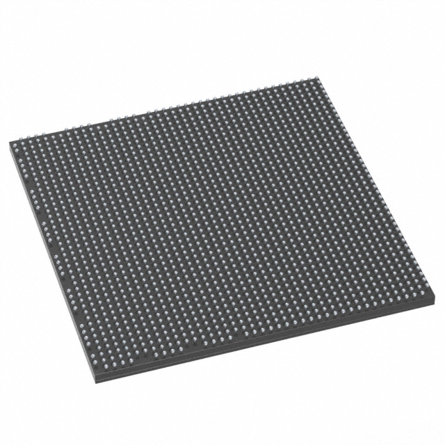
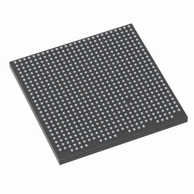
Virtex®-5 SXT Field Programmable Gate Array (FPGA) IC 360 3096576 34816 665-BBGA, FCBGA |
|---|---|
| Quantity | 1,548 Available (as of June 15, 2026) |

| Product Category | Field Programmable Gate Array (FPGA) |
|---|---|
| Manufacturer | AMD |
| Manufacturing Status | Obsolete |
| Manufacturer Standard Lead Time | Contact Us |
| Datasheet |
Specifications & Environmental
| Device Package | 665-FCBGA (27x27) | Grade | Commercial | Operating Temperature | 0°C – 85°C | ||
|---|---|---|---|---|---|---|---|
| Package / Case | 665-BBGA, FCBGA | Number of I/O | 360 | Voltage | 950 mV - 1.05 V | ||
| Mounting Method | Surface Mount | RoHS Compliance | Unknown | REACH Compliance | REACH Unaffected | ||
| Moisture Sensitivity Level | 4 (72 Hours) | Number of LABs/CLBs | 2720 | Number of Logic Elements/Cells | 34816 | ||
| Number of Gates | N/A | ECCN | 3A991D | HTS Code | 8542.39.0001 | ||
| Qualification | N/A | Total RAM Bits | 3096576 |
Overview of XC5VSX35T-1FFG665CES – Virtex®-5 SXT Field Programmable Gate Array (FPGA), 665-FCBGA (27×27)
The XC5VSX35T-1FFG665CES is a Virtex®-5 SXT Field Programmable Gate Array (FPGA) IC from AMD designed for commercial programmable-logic applications. It combines a large logic capacity with substantial on-chip memory and a high-pin-count I/O footprint to address demanding integration and I/O aggregation requirements.
Key architectural attributes include approximately 34,816 logic elements, roughly 3.1 Mbits of embedded memory, and 360 user I/O pins, all packaged in a 665-ball FCBGA for surface-mount assembly.
Key Features
- Logic Capacity Approximately 34,816 logic elements to implement complex custom digital functions and control logic.
- Embedded Memory Approximately 3.1 Mbits of on-chip RAM for data buffering, state storage, and algorithm working memory.
- I/O Resources 360 user I/O pins suitable for high-density interfacing and multi-channel connectivity.
- Core Power Core supply voltage range of 950 mV to 1.05 V to match system power domains and enable standard power sequencing.
- Package and Mounting 665-ball FCBGA package (665-FCBGA, 27×27) in a surface-mount form factor for compact board-level integration.
- Operating Range Commercial-grade operating temperature range of 0 °C to 85 °C, suitable for a wide range of commercial electronic products.
- Standards Compliance RoHS‑compliant construction for regulatory and environmental conformity.
Typical Applications
- High-density I/O Interfaces Use the 360 user I/O pins to consolidate multiple peripheral and signal interfaces on a single programmable device.
- Custom Digital Processing Leverage the ~34,816 logic elements to implement bespoke state machines, protocol handling, and data-path logic.
- On-chip Data Buffering Utilize approximately 3.1 Mbits of embedded RAM for packet buffering, frame storage, or intermediate data staging.
Unique Advantages
- Significant Programmable Capacity: Approximately 34,816 logic elements enable implementation of large, custom digital designs without external logic devices.
- Integrated Memory: Roughly 3.1 Mbits of on-chip RAM reduces reliance on external memory for many buffering and storage tasks, simplifying BOM and board layout.
- High I/O Count: 360 user I/Os support dense connectivity and multi-channel interfacing, lowering the need for additional I/O expanders.
- Compact Surface-Mount Package: The 665-FCBGA (27×27) package provides a high pin count in a compact footprint for space-constrained boards.
- Commercial Temperature Range: Rated 0 °C to 85 °C for reliable operation in commercial electronic environments.
- RoHS Compliance: Environmentally compliant construction supports regulatory requirements for electronic assemblies.
Why Choose XC5VSX35T-1FFG665CES?
The XC5VSX35T-1FFG665CES positions itself as a capable commercial-grade FPGA option where substantial programmable logic, embedded memory, and a high I/O count are required in a compact surface-mount package. Its combination of logic elements, on-chip RAM, and 360 user I/Os makes it suitable for designs that demand integrated digital processing and dense interfacing while maintaining a manageable bill of materials.
This device is well-suited to engineering teams building commercial electronic products that need scalable programmable logic, on-board memory resources, and a high-pin-count package backed by AMD's Virtex‑5 family pedigree.
If you would like pricing or availability for the XC5VSX35T-1FFG665CES, request a quote or submit an inquiry to receive a formal quotation and lead-time information.


Date Founded: 1969
Headquarters: Santa Clara, California, USA
Employees: 25,000+
Revenue: $22.68 Billion
Certifications and Memberships: ISO9001:2015, RoHS, REACH


