
XC7K480T-L2FFG901E
| Part Description |
Kintex®-7 Field Programmable Gate Array (FPGA) IC 380 35205120 477760 900-BBGA, FCBGA |
|---|---|
| Quantity | 481 Available (as of June 15, 2026) |
| Product Category | Field Programmable Gate Array (FPGA) |
|---|---|
| Manufacturer | AMD |
| Manufacturing Status | Active |
| Manufacturer Standard Lead Time | 16 Weeks |
| Datasheet |
Specifications & Environmental
| Device Package | 901-FCBGA (31x31) | Grade | Extended | Operating Temperature | 0°C – 100°C | ||
|---|---|---|---|---|---|---|---|
| Package / Case | 900-BBGA, FCBGA | Number of I/O | 380 | Voltage | 870 mV - 930 mV | ||
| Mounting Method | Surface Mount | RoHS Compliance | ROHS3 Compliant | REACH Compliance | REACH Unaffected | ||
| Moisture Sensitivity Level | 4 (72 Hours) | Number of LABs/CLBs | 37325 | Number of Logic Elements/Cells | 477760 | ||
| Number of Gates | N/A | ECCN | 3A991D | HTS Code | 8542.39.0001 | ||
| Qualification | N/A | Total RAM Bits | 35205120 |
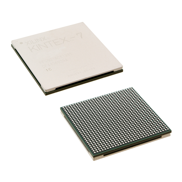
Overview of XC7K480T-L2FFG901E – Kintex®-7 Field Programmable Gate Array (FPGA), 900‑BBGA
The XC7K480T-L2FFG901E is a Kintex®-7 Field Programmable Gate Array (FPGA) IC offering large-scale programmable logic in a compact 900‑BBGA package. It provides 477,760 logic elements, approximately 35.2 Mbits of embedded memory, and 380 user I/O pins for high-density designs.
Packaged as a 901‑FCBGA (31×31) surface-mount device with extended grade components, the device operates from a core supply of 870 mV to 930 mV and an ambient range of 0 °C to 100 °C, making it suitable for systems that require substantial on-chip resources in a single FPGA device.
Key Features
- Core Logic 477,760 logic elements and 37,325 CLBs provide the programmable fabric required for large-scale digital designs.
- Embedded Memory Approximately 35.2 Mbits of on-chip RAM for buffering, FIFOs, and data storage directly within the FPGA fabric.
- I/O Capacity 380 user I/O pins support extensive external interfacing and connectivity options from a single device.
- Package 900‑BBGA / 901‑FCBGA (31×31) surface-mount package delivers a high-pin-count, compact footprint for board-level integration.
- Power Core voltage supply range of 870 mV to 930 mV enables defined power sequencing and supply design around the FPGA core.
- Operating Range Extended grade device specified for ambient operation from 0 °C to 100 °C.
- Mounting Surface-mount FCBGA package intended for modern PCB assembly and automated placement processes.
- RoHS Compliance Device is RoHS compliant.
Typical Applications
- High-density logic implementations — Leverage the large logic element count and CLB resources for complex digital designs that require extensive programmable fabric.
- On-chip data buffering and memory-intensive tasks — Use the approximately 35.2 Mbits of embedded RAM for frame buffering, packet storage, and internal data handling.
- Multi‑I/O interface systems — 380 I/O pins support designs that require numerous external interfaces or parallel data paths.
Unique Advantages
- High logic capacity: 477,760 logic elements and 37,325 CLBs provide ample resources to implement large, complex designs without partitioning across multiple devices.
- Substantial embedded memory: Approximately 35.2 Mbits of on-chip RAM reduces dependence on external memory and simplifies board-level memory architectures.
- Extensive I/O provision: 380 user I/O pins enable wide connectivity options and support dense peripheral interfacing from a single package.
- Compact, high‑pin‑count package: 900‑BBGA / 901‑FCBGA (31×31) delivers a balance of density and manufacturability for space-constrained PCBs.
- Defined power and thermal characteristics: Core supply range of 870–930 mV and operating range of 0 °C to 100 °C support predictable system power and thermal planning.
- RoHS compliant: Meets RoHS requirements for environmentally conscious designs.
Why Choose XC7K480T-L2FFG901E?
The XC7K480T-L2FFG901E combines a very large logic fabric, significant on-chip memory, and broad I/O capability in a single extended‑grade FCBGA package, enabling consolidation of complex system functions into one FPGA. Its defined core voltage range and operating temperature window make it suitable for designs that need predictable power and environmental behavior.
This device is well suited for engineering teams seeking a high-capacity, tightly integrated FPGA solution that reduces board-level complexity and supports scalable designs with substantial internal resources.
Request a quote or submit a pricing inquiry to check availability and obtain delivery and pricing details for the XC7K480T-L2FFG901E.


Date Founded: 1969
Headquarters: Santa Clara, California, USA
Employees: 25,000+
Revenue: $22.68 Billion
Certifications and Memberships: ISO9001:2015, RoHS, REACH


