
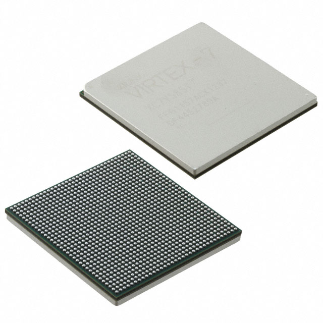
XC7VX690T-1FFG1930C
| Part Description |
Virtex®-7 XT Field Programmable Gate Array (FPGA) IC 1000 54190080 693120 1924-BBGA, FCBGA |
|---|---|
| Quantity | 257 Available (as of June 15, 2026) |

| Product Category | Field Programmable Gate Array (FPGA) |
|---|---|
| Manufacturer | AMD |
| Manufacturing Status | Active |
| Manufacturer Standard Lead Time | 16 Weeks |
| Datasheet |
Specifications & Environmental
| Device Package | 1930-FCBGA (45x45) | Grade | Commercial | Operating Temperature | 0°C – 85°C | ||
|---|---|---|---|---|---|---|---|
| Package / Case | 1924-BBGA, FCBGA | Number of I/O | 1000 | Voltage | 970 mV - 1.03 V | ||
| Mounting Method | Surface Mount | RoHS Compliance | ROHS3 Compliant | REACH Compliance | REACH Unaffected | ||
| Moisture Sensitivity Level | 4 (72 Hours) | Number of LABs/CLBs | 54150 | Number of Logic Elements/Cells | 693120 | ||
| Number of Gates | N/A | ECCN | 3A001A7A | HTS Code | 8542.39.0001 | ||
| Qualification | N/A | Total RAM Bits | 54190080 |
Overview of XC7VX690T-1FFG1930C – Virtex®-7 XT FPGA, 1930-FCBGA
The XC7VX690T-1FFG1930C is a Virtex®-7 XT Field Programmable Gate Array (FPGA) from AMD designed for high-density, configurable digital logic and embedded memory applications. With a large logic element count, substantial on-chip RAM, and a high I/O count, this device targets designs that require significant integration of logic, memory, and interface connectivity within a surface-mount FCBGA package.
Its specification set positions the device for systems that need substantial programmable resources and high pin-count connectivity while operating within a commercial temperature range and low-voltage core supply window.
Key Features
- Core & Logic Capacity — 693,120 logic elements and 54,150 configurable logic blocks (CLBs) provide extensive programmable fabric for complex designs and large-scale integration.
- On-chip Memory — Approximately 54 Mbits of embedded RAM (54,190,080 bits) to support memory-intensive algorithms, buffering, and on-chip data storage.
- I/O Density — Up to 1,000 I/O pins to accommodate high-signal-count interfaces, multi-channel connectivity, and broad peripheral integration.
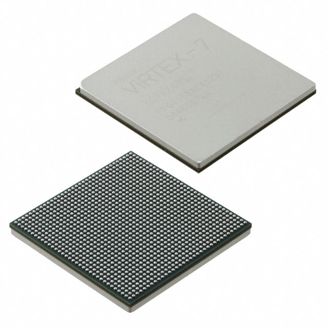
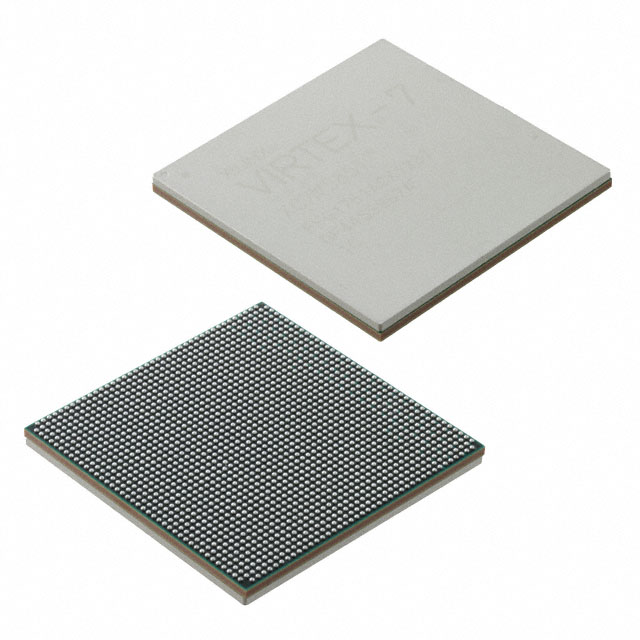
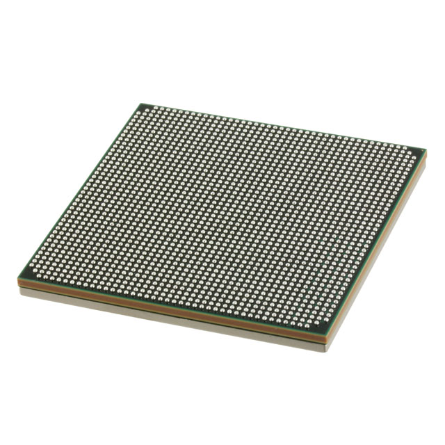
- Package & Mounting — Supplier device package: 1930-FCBGA (45×45). Package case listed as 1924-BBGA, FCBGA. Designed for surface-mount assembly.
- Power Supply — Core voltage range of 0.970 V to 1.030 V, enabling designs that align with the device’s low-voltage core requirements.
- Temperature & Grade — Commercial grade operation from 0 °C to 85 °C for standard commercial applications and environments.
- Environmental Compliance — RoHS compliant, supporting regulatory requirements for lead-free assembly.
Typical Applications
- High-density system design — Large programmable fabric supports complex logic implementations and system consolidation where thousands of logic elements are required.
- Memory-intensive embedded processing — Approximately 54 Mbits of on-chip RAM makes the device suitable for buffering, packet processing, and other workloads that rely on embedded memory.
- High I/O interface systems — Up to 1,000 I/O pins enable interfacing to many peripherals, multi-channel data acquisition, and high-bandwidth communication front-ends.
Unique Advantages
- High logic density: 693,120 logic elements offer extensive programmable resources to implement large, integrated digital systems on a single FPGA.
- Substantial embedded memory: Approximately 54 Mbits of on-chip RAM reduces external memory dependencies and improves data-path performance for memory-heavy designs.
- Extensive I/O capability: 1,000 I/O pins simplify multi-interface designs and reduce the need for external multiplexing or expanders.
- Surface-mount FCBGA packaging: 1930-FCBGA (45×45) supplier package supports high-pin-count board layouts and compact system integration.
- Commercial temperature rating: Operation from 0 °C to 85 °C aligns with mainstream commercial deployments and standard electronic assemblies.
- RoHS compliance: Enables use in lead-free manufacturing processes and supports regulatory requirements.
Why Choose XC7VX690T-1FFG1930C?
The XC7VX690T-1FFG1930C delivers a combination of high logic capacity, substantial embedded memory, and large I/O count within an FCBGA surface-mount package, making it well suited to designs that consolidate multiple functions into a single FPGA. Its specification set is tailored for engineers and procurement teams looking for a commercially graded Virtex‑7 family device with significant programmable resources.
For projects that demand scalable logic resources, on-chip memory for performance-sensitive paths, and broad connectivity, this Virtex‑7 XT device provides a robust platform to reduce external component count and simplify board-level integration.
Request a quote or submit a procurement inquiry to check pricing and availability for the XC7VX690T-1FFG1930C.


Date Founded: 1969
Headquarters: Santa Clara, California, USA
Employees: 25,000+
Revenue: $22.68 Billion
Certifications and Memberships: ISO9001:2015, RoHS, REACH


