
XCV100E-7PQ240I
| Part Description |
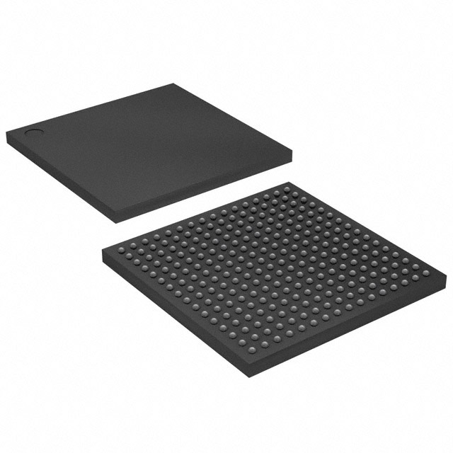
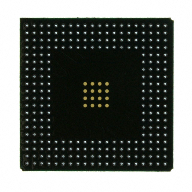
Virtex®-E Field Programmable Gate Array (FPGA) IC 158 81920 2700 240-BFQFP |
|---|---|
| Quantity | 449 Available (as of October 8, 2026) |

| Product Category | Field Programmable Gate Array (FPGA) |
|---|---|
| Manufacturer | AMD |
| Manufacturing Status | Obsolete |
| Manufacturer Standard Lead Time | Contact Us |
| Datasheet |
Specifications & Environmental
| Device Package | 240-PQFP (32x32) | Grade | Industrial | Operating Temperature | -40°C – 100°C | ||
|---|---|---|---|---|---|---|---|
| Package / Case | 240-BFQFP | Number of I/O | 158 | Voltage | 1.71 V - 1.89 V | ||
| Mounting Method | Surface Mount | RoHS Compliance | RoHS non-compliant | REACH Compliance | REACH Unaffected | ||
| Moisture Sensitivity Level | 3 (168 Hours) | Number of LABs/CLBs | 600 | Number of Logic Elements/Cells | 2700 | ||
| Number of Gates | 128236 | ECCN | EAR99 | HTS Code | 8542.39.0001 | ||
| Qualification | N/A | Total RAM Bits | 81920 |
Overview of XCV100E-7PQ240I – Virtex®-E FPGA, 240-BFQFP, Industrial
The XCV100E-7PQ240I is an industrial‑grade Virtex®-E field programmable gate array offered in a 240‑BFQFP surface‑mount package. It integrates 2,700 logic elements, approximately 0.08 Mbits of embedded memory (81,920 bits), and 158 I/O pins to address demanding interface and control applications.
Designed on the Virtex‑E 1.8 V family architecture, this device targets applications requiring flexible high‑performance I/O, on‑chip RAM resources, and built‑in clock management while operating across an industrial temperature range and RoHS‑compliant manufacturing.
Key Features
- Logic Density 2,700 logic elements providing 128,236 equivalent gates for implementing custom digital logic and control functions.
- Embedded Memory Approximately 81,920 bits (≈0.08 Mbits) of on‑chip RAM for buffering, small LUT RAMs, and fast local storage.
- I/O and Interface Support 158 I/O pins with SelectI/O‑class flexibility described for the Virtex‑E family, including support for multiple high‑performance differential and single‑ended standards.
- Clock Management Family features include multiple digital delay‑locked loops (DLLs) and support for high‑frequency LVPECL/LVDS clock inputs as described in the Virtex‑E datasheet.
- External Memory Interfaces Virtex‑E family methods and SelectRAM+ memory hierarchy support high‑speed connections to external memories such as DDR SDRAM and ZBT SRAM (per datasheet capabilities).
- Power and Supply Internal VCCINT supply range of 1.71 V to 1.89 V consistent with the 1.8 V Virtex‑E family process.
- Packaging and Mounting 240‑pin BFQFP package (supplier device package: 240‑PQFP 32×32) for surface‑mount PCB assembly.
- Industrial Temperature Range Rated for operation from −40 °C to 100 °C, suitable for industrial environments.
- Compliance and Test RoHS‑compliant and indicated as 100% factory tested in the Virtex‑E product specification.
Typical Applications
- High‑speed I/O Bridging Protocol translators and interface adapters that leverage flexible I/O standards and the device’s I/O count to connect disparate systems.
- Memory Interface and Controllers Custom controllers and buffering logic for external DDR SDRAM or ZBT SRAM leveraging the Virtex‑E memory hierarchy capabilities.
- Industrial Control Systems Custom logic for motor control, machine I/O aggregation, and process automation operating across an industrial temperature range.
- Signal Conditioning and Processing Front‑end data handling and pre‑processing for systems requiring configurable logic and local RAM buffering.
Unique Advantages
- Flexible, multi‑standard I/O: Supports a wide set of single‑ended and differential signaling options as described for the Virtex‑E family, enabling diverse interface implementations.
- Balanced resource mix: Combination of 2,700 logic elements and on‑chip RAM provides a compact platform for mid‑range custom logic and buffering tasks.
- Industrial reliability: Rated for −40 °C to 100 °C and RoHS‑compliant, suitable for deployment in industrial environments.
- Robust clocking options: Built‑in DLLs and support for high‑speed differential clock inputs (per family datasheet) simplify timing and clock distribution for high‑performance designs.
- Proven family features: Leverages Virtex‑E family capabilities such as SelectRAM+ memory hierarchy and SelectI/O technology as documented in the product specification.
Why Choose XCV100E-7PQ240I?
The XCV100E-7PQ240I provides a compact, industrial‑rated FPGA solution that pairs mid‑range logic density with flexible I/O and on‑chip memory to implement custom interfaces, memory controllers, and control logic. Its 240‑pin BFQFP package and surface‑mount mounting make it suitable for board‑level integration in space‑constrained industrial designs.
Engineers choosing this Virtex‑E device benefit from family‑level capabilities—multi‑standard I/O support, digital clock management, and a documented memory hierarchy—backed by factory testing and RoHS compliance for production deployment.
Request a quote or submit a purchase inquiry to receive pricing and availability for the XCV100E-7PQ240I. Our team will provide the information needed to evaluate integration and lead times.






















Date Founded: 1969
Headquarters: Santa Clara, California, USA
Employees: 25,000+
Revenue: $22.68 Billion
Certifications and Memberships: ISO9001:2015, RoHS, REACH











