
XCV100E-8FG256C
| Part Description |
Virtex®-E Field Programmable Gate Array (FPGA) IC 176 81920 2700 256-BGA |
|---|---|
| Quantity | 544 Available (as of June 16, 2026) |
| Product Category | Field Programmable Gate Array (FPGA) |
|---|---|
| Manufacturer | AMD |
| Manufacturing Status | Obsolete |
| Manufacturer Standard Lead Time | Contact Us |
| Datasheet |
Specifications & Environmental
| Device Package | 256-FBGA (17x17) | Grade | Commercial | Operating Temperature | 0°C – 85°C | ||
|---|---|---|---|---|---|---|---|
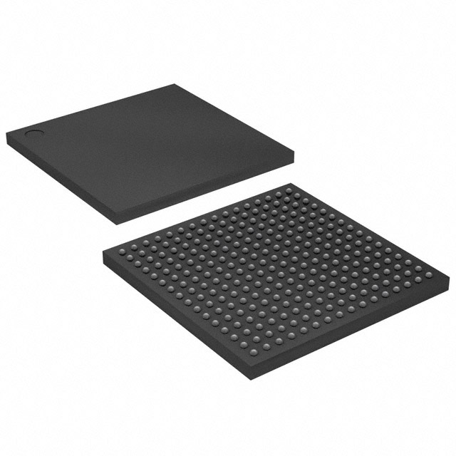
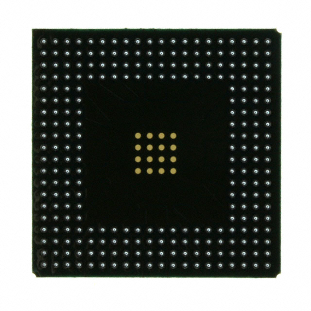
| Package / Case | 256-BGA | Number of I/O | 176 | Voltage | 1.71 V - 1.89 V | ||
| Mounting Method | Surface Mount | RoHS Compliance | RoHS non-compliant | REACH Compliance | REACH Unaffected | ||
| Moisture Sensitivity Level | 3 (168 Hours) | Number of LABs/CLBs | 600 | Number of Logic Elements/Cells | 2700 | ||
| Number of Gates | 128236 | ECCN | EAR99 | HTS Code | 8542.39.0001 | ||
| Qualification | N/A | Total RAM Bits | 81920 |
Overview of XCV100E-8FG256C – Virtex®-E FPGA, 256-BGA, 176 I/O
The XCV100E-8FG256C is a Virtex®-E family field programmable gate array (FPGA) in a 256-ball BGA package. It provides reprogrammable logic with substantial I/O density and on-chip RAM, suitable for designs that require flexible, in-system configurable digital logic and moderate gate and memory resources.
Built on the Virtex-E architecture, this device combines a 1.8 V core voltage range, a broad set of family-level interface capabilities, and commercial-grade operating conditions for embedded and electronic system designs.
Key Features
- Logic and Gates Approximately 2,700 logic elements supporting about 128,236 gates for mid-density logic integration and custom digital functions.
- Embedded Memory Approximately 81,920 bits of on-chip RAM for buffering, state storage, and small FIFOs directly inside the FPGA fabric.
- I/O Capacity 176 user I/Os provide extensive external connectivity from a single device footprint.
- Power Supply Core supply specified at 1.71 V to 1.89 V, aligning with the Virtex-E 1.8 V family architecture.
- Package and Mounting 256-ball BGA (256-FBGA, 17×17) in a surface-mount package ideal for board-level integration where a high-pin-count, compact footprint is required.
- Operating Range Commercial temperature grade with an operating range of 0 °C to 85 °C.
- Regulatory RoHS compliant for lead-free assembly processes.
- Virtex‑E Family Capabilities Series-level features include fast 1.8 V architecture, advanced SelectI/O+ I/O technology, differential signaling support (LVDS, BLVDS, LVPECL), SelectRAM+ memory hierarchy, and built-in clock management with multiple DLLs — enabling a wide range of interface and timing configurations.
Typical Applications
- High‑density I/O Interfaces Use the 176 I/Os to implement interface bridging, protocol adaptation, or custom front-end logic where multiple signals and standards must be supported.
- Embedded Logic and Control Leverage the device’s logic elements and on-chip RAM for control algorithms, state machines, and custom processing blocks in embedded systems.
- Memory Buffering and Glue Logic On-chip RAM and reprogrammability make this FPGA suitable for buffering, bus conversion, and glue logic between different system components.
- Prototyping and In‑System Reconfiguration SRAM-based, reprogrammable architecture supports iterative development and in-system updates for evolving designs.
Unique Advantages
- Balanced Mid‑Density Solution: Offers a combination of logic, gates, and on-chip RAM suitable for designs that need more than small CPLDs but do not require very high gate counts.
- Substantial I/O in a Compact Package: 176 I/Os in a 256-FBGA (17×17) package reduce board complexity while preserving routing flexibility.
- Family-Level Interface Flexibility: Virtex‑E SelectI/O+ and differential signaling support allow implementation of multiple I/O standards for mixed-signal system designs.
- Commercial Temperature and RoHS Compliance: Commercial operating range (0 °C to 85 °C) and RoHS compliance simplify integration into mainstream electronic products and assembly processes.
- Surface Mount Form Factor: Surface-mount 256-BGA simplifies automated PCB assembly and supports higher-density board designs.
Why Choose XCV100E-8FG256C?
The XCV100E-8FG256C positions itself as a practical Virtex‑E FPGA option for designers needing reprogrammable logic with a meaningful complement of I/O and embedded memory in a compact BGA package. Its 1.8 V core, family-level I/O and clock-management features, and commercial-grade temperature range make it well suited to embedded systems, interface logic, and prototyping tasks where flexibility and moderate integration density are priorities.
With RoHS compliance and a surface-mount 256-FBGA footprint, this part addresses modern assembly requirements while providing access to the Virtex‑E family’s development ecosystem and series-level capabilities for clocking, I/O standards, and on-chip memory architectures.
Request a quote or submit an inquiry to receive pricing and availability for XCV100E-8FG256C and to discuss how this Virtex‑E FPGA can fit into your next design.


Date Founded: 1969
Headquarters: Santa Clara, California, USA
Employees: 25,000+
Revenue: $22.68 Billion
Certifications and Memberships: ISO9001:2015, RoHS, REACH


