
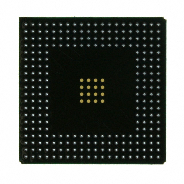
XCV150-4FG256I
| Part Description |
Virtex® Field Programmable Gate Array (FPGA) IC 176 49152 3888 256-BGA |
|---|---|
| Quantity | 1,612 Available (as of June 15, 2026) |

| Product Category | Field Programmable Gate Array (FPGA) |
|---|---|
| Manufacturer | AMD |
| Manufacturing Status | Obsolete |
| Manufacturer Standard Lead Time | Contact Us |
| Datasheet |
Specifications & Environmental
| Device Package | 256-FBGA (17x17) | Grade | Industrial | Operating Temperature | -40°C – 100°C | ||
|---|---|---|---|---|---|---|---|
| Package / Case | 256-BGA | Number of I/O | 176 | Voltage | 2.375 V - 2.625 V | ||
| Mounting Method | Surface Mount | RoHS Compliance | RoHS non-compliant | REACH Compliance | REACH Unaffected | ||
| Moisture Sensitivity Level | 3 (168 Hours) | Number of LABs/CLBs | 864 | Number of Logic Elements/Cells | 3888 | ||
| Number of Gates | 164674 | ECCN | EAR99 | HTS Code | 8542.39.0001 | ||
| Qualification | N/A | Total RAM Bits | 49152 |
Overview of XCV150-4FG256I – Virtex® Field Programmable Gate Array (FPGA), 176 I/O, 3,888 logic elements, 256‑BGA
The XCV150-4FG256I is an industrial-grade Virtex® FPGA in a 256‑BGA package, offering a balanced combination of programmable logic, embedded memory, and flexible I/O for embedded and industrial designs. It is an SRAM-based, reprogrammable device that suits applications requiring in-system configuration, multi-standard I/O, and robust operating ranges.
Key architecture elements include thousands of logic elements, on-chip RAM, multiple clock management resources and multi-standard SelectIO interfaces—making the device appropriate for communications, industrial control, and high-performance embedded systems.
Key Features
- Logic Resources — 3,888 logic elements organized into 864 CLBs, providing gate-equivalent density suitable for medium-complexity FPGA designs.
- Embedded Memory — 49,152 total RAM bits of on-chip memory for data buffering, small lookup tables, and fast local storage.
- I/O and Interfaces — 176 user I/O pins with multi-standard SelectIO support for a wide range of interface signaling options and direct connectivity to high-performance memory devices as described in the Virtex family documentation.
- Clock Management — Built-in clock-management circuitry includes multiple dedicated delay-locked loops (DLLs) and hierarchical global/local clock nets to support advanced clock control and low-skew distribution.
- Configuration and Reprogramming — SRAM-based in-system configuration supports unlimited re-programmability and multiple programming modes for flexible deployment and field updates.
- Dedicated Arithmetic Resources — Architecture includes dedicated carry logic and multiplier support for efficient implementation of arithmetic and DSP functions.
- Package and Mounting — 256‑FBGA (17×17) package, surface-mount, designed for compact board-level integration.
- Power and Temperature — Operates from a core supply range of 2.375 V to 2.625 V and specified for an industrial temperature range of −40 °C to 100 °C.
- Compliance — RoHS compliant.
Typical Applications
- Industrial Automation — Implement real-time control logic, sensor interfacing, and deterministic I/O aggregation within industrial temperature ranges.
- Communications Equipment — Use the multi-standard I/O and on-chip memory for protocol bridging, packet buffering, and custom interface logic in telecom or networking gear.
- PCI-based Systems — Suitable for designs that integrate with PCI or Compact PCI environments where hot‑swap and PCI‑compliant interfaces are required by system architecture.
- Embedded Processing — Accelerate custom data paths and offload compute tasks using dedicated arithmetic resources and configurable memory structures.
Unique Advantages
- Reprogrammable Hardware: SRAM-based configuration enables unlimited in-system updates and flexible prototyping or production changes without mask revisions.
- Balanced Resource Mix: Combination of 3,888 logic elements and 49,152 bits of embedded RAM supports medium-density logic with on-chip storage to reduce external memory dependence.
- Advanced Clocking: Multiple DLLs and hierarchical clock nets simplify clock-domain management for timing-sensitive designs.
- Robust Environmental Range: Industrial-grade specification and an operating temperature range of −40 °C to 100 °C for deployment in challenging environments.
- Compact, Surface-Mount Package: 256‑FBGA (17×17) package enables high I/O count in a compact footprint for space-constrained boards.
- Vendor Ecosystem: Supported by the Virtex family feature set for established design flows and configuration modes to streamline development and deployment.
Why Choose XCV150-4FG256I?
The XCV150-4FG256I positions itself as a versatile mid-range Virtex FPGA that combines a practical logic capacity with embedded memory and extensive I/O in a compact 256‑BGA package. Its industrial temperature rating and RoHS compliance make it suitable for production systems that require dependable operation across a wide temperature span.
This device is well matched to engineers designing communications modules, industrial controllers, and embedded platforms that need reprogrammable logic, on-chip memory, robust clocking, and multi-standard I/O support while maintaining a compact board footprint.
Request a quote or submit an RFQ to check availability and lead time for the XCV150-4FG256I and evaluate how this Virtex FPGA fits your next design.


Date Founded: 1969
Headquarters: Santa Clara, California, USA
Employees: 25,000+
Revenue: $22.68 Billion
Certifications and Memberships: ISO9001:2015, RoHS, REACH


