
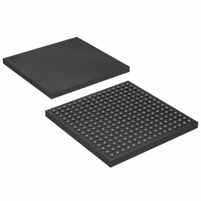
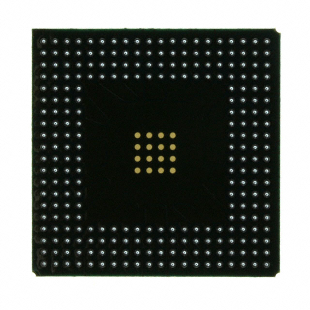
XCV150-4FG256C
| Part Description |
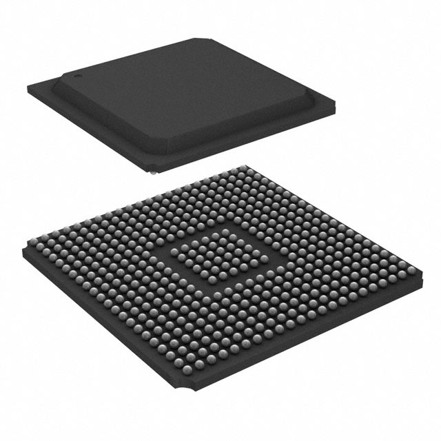
Virtex® Field Programmable Gate Array (FPGA) IC 176 49152 3888 256-BGA |
|---|---|
| Quantity | 1,061 Available (as of October 8, 2026) |
| Product Category | Field Programmable Gate Array (FPGA) |
|---|---|
| Manufacturer | AMD |
| Manufacturing Status | Obsolete |
| Manufacturer Standard Lead Time | Contact Us |
| Datasheet |
Specifications & Environmental
| Device Package | 256-FBGA (17x17) | Grade | Commercial | Operating Temperature | 0°C – 85°C | ||
|---|---|---|---|---|---|---|---|
| Package / Case | 256-BGA | Number of I/O | 176 | Voltage | 2.375 V - 2.625 V | ||
| Mounting Method | Surface Mount | RoHS Compliance | RoHS non-compliant | REACH Compliance | REACH Unaffected | ||
| Moisture Sensitivity Level | 3 (168 Hours) | Number of LABs/CLBs | 864 | Number of Logic Elements/Cells | 3888 | ||
| Number of Gates | 164674 | ECCN | EAR99 | HTS Code | 8542.39.0001 | ||
| Qualification | N/A | Total RAM Bits | 49152 |
Overview of XCV150-4FG256C – Virtex® Field Programmable Gate Array (FPGA) IC 176 49152 3888 256-BGA
The XCV150-4FG256C is an SRAM-based Virtex FPGA delivering programmable logic with a balance of capacity and system-level I/O. This commercial-grade device provides 3,888 logic elements, approximately 49 Kbits of embedded RAM, and support for multi-standard I/O and clock management features suitable for a wide range of high-performance digital designs.
Designed for surface-mount applications in a 256-BGA (256-FBGA, 17×17) package, the device is RoHS compliant and operates from a 2.375 V to 2.625 V supply within a 0 °C to 85 °C temperature range.
Key Features
- Core Density — Approximately 3,888 logic elements and 164,674 system gates provide mid-range programmable logic capacity for complex glue logic, custom state machines, and moderate-scale datapaths.
- Embedded Memory — Approximately 49,152 bits of on-chip RAM support LUT-based RAM configurations and small embedded buffers for data storage and packet buffering.
- I/O and Packaging — 176 I/O pins in a 256-BGA (256-FBGA, 17×17) surface-mount package enable dense board-level connectivity while minimizing PCB footprint.
- Clock Management — Family-level clock features include multiple dedicated delay-locked loops (DLLs) and global/local clock networks to support precise clock distribution and low-skew designs.
- Configurable Logic and Arithmetic Support — Architecture includes dedicated carry logic, multiplier support, cascade chains, and abundant registers with clock enable and set/reset options for arithmetic and control applications.
- In-System Configuration — SRAM-based device supports multiple programming modes for in-system configuration and unlimited reprogramming during development and prototyping.
- Power and Environment — Operates from 2.375 V to 2.625 V supply range; commercial operating temperature range from 0 °C to 85 °C.
- Standards and Test — 100% factory tested and includes IEEE 1149.1 boundary-scan for board-level testability; RoHS compliant.
Typical Applications
- Embedded Control and Glue Logic — Implement custom control functions, protocol converters, and board-level glue logic where reprogrammability and moderate logic density are required.
- Signal Processing and Arithmetic Blocks — Use dedicated carry and multiplier resources for fixed-point DSP blocks, filtering, and accumulator functions within larger systems.
- Prototyping and Development — SRAM-based configuration enables rapid iteration and in-system reprogramming for hardware validation and prototype platforms.
- PCI and Legacy System Interfaces — Family features include PCI-compliant operation and Compact PCI hot-swap support, suitable for legacy peripheral and backplane interface designs.
Unique Advantages
- Balanced Capacity and I/O: 3,888 logic elements and 176 I/O provide a mid-range combination that simplifies integration of moderate-complexity designs without excessive board-level components.
- Flexible Memory Options: Approximately 49 Kbits of embedded RAM and LUT-configurable RAM modes let you implement small FIFOs, buffers, and state storage without external memory.
- Robust Clocking Resources: Multiple DLLs and hierarchical clock networks enable precise timing control across complex logic blocks, reducing clock skew and easing timing closure.
- In-System Reprogrammability: SRAM-based configuration supports unlimited reprogramming and multiple programming modes for design updates and field-level revisions.
- Board-Level Testability: IEEE 1149.1 boundary-scan and 100% factory testing improve manufacturability and debug efficiency during bring-up.
- Compact, SMT Package: 256-FBGA (17×17) surface-mount package supports high-density PCB layouts while maintaining a standard footprint for assembly.
Why Choose XCV150-4FG256C?
The XCV150-4FG256C positions itself as a practical, reprogrammable logic solution for designers needing a mid-range FPGA with a strong mix of logic resources, embedded memory, and I/O. Its Virtex architecture provides dedicated arithmetic and clocking features that simplify implementation of performance-sensitive functions while the SRAM configuration model supports ongoing iteration and system updates.
This part is well suited to design teams building prototypes, subsystem controllers, and interface logic that require commercial-grade reliability, compact packaging, and a proven feature set for timing, memory, and I/O management.
Request a quote or submit a procurement inquiry to evaluate the XCV150-4FG256C for your next design project.





















Date Founded: 1969
Headquarters: Santa Clara, California, USA
Employees: 25,000+
Revenue: $22.68 Billion
Certifications and Memberships: ISO9001:2015, RoHS, REACH











