
XCV400-4BG560I
| Part Description |
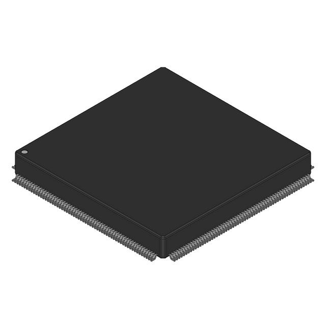
Virtex® Field Programmable Gate Array (FPGA) IC 404 81920 10800 560-LBGA Exposed Pad, Metal |
|---|---|
| Quantity | 1,135 Available (as of June 10, 2026) |

| Product Category | Field Programmable Gate Array (FPGA) |
|---|---|
| Manufacturer | AMD |
| Manufacturing Status | Obsolete |
| Manufacturer Standard Lead Time | Contact Us |
| Datasheet |
Specifications & Environmental
| Device Package | 560-MBGA (42.5x42.5) | Grade | Industrial | Operating Temperature | -40°C – 100°C | ||
|---|---|---|---|---|---|---|---|
| Package / Case | 560-LBGA Exposed Pad, Metal | Number of I/O | 404 | Voltage | 2.375 V - 2.625 V | ||
| Mounting Method | Surface Mount | RoHS Compliance | RoHS non-compliant | REACH Compliance | REACH Unaffected | ||
| Moisture Sensitivity Level | 3 (168 Hours) | Number of LABs/CLBs | 2400 | Number of Logic Elements/Cells | 10800 | ||
| Number of Gates | 468252 | ECCN | 3A991D | HTS Code | 8542.39.0001 | ||
| Qualification | N/A | Total RAM Bits | 81920 |
Overview of XCV400-4BG560I – Virtex FPGA, 404 I/O, 10,800 Logic Cells, 560-LBGA
The XCV400-4BG560I is an SRAM-based Virtex field programmable gate array (FPGA) optimized for high-capacity, high-performance programmable logic designs. This industrial-grade device integrates 10,800 logic cells across 2,400 CLBs with 81,920 bits of embedded RAM and 404 user I/O, delivering a versatile platform for complex system designs that require reprogrammability and flexible I/O.
Its architecture combines dedicated arithmetic resources, hierarchical on-chip memory, multi-standard I/O support and advanced clock-management features to address applications where configurable logic density, deterministic timing and broad interfacing are required.
Key Features
- Core Capacity — 10,800 logic cells across 2,400 CLBs and approximately 468,252 system gates provide substantial programmable logic for medium-to-high complexity designs.
- Embedded Memory — 81,920 total RAM bits (approximately 0.082 Mbits) for LUT-configurable RAM, dual-ported RAM and shift-register implementations.
- I/O and Interface Flexibility — 404 user I/O pins and multi-standard SelectIO support (16 interface standards) for broad external memory and peripheral interfacing.
- Clock Management — Four dedicated delay-locked loops (DLLs) with four primary low-skew global clock distribution nets and 24 secondary local clock nets for refined timing control.
- Arithmetic and Logic Resources — Dedicated carry logic and multiplier support for high-speed arithmetic and wide-input functions.
- Configuration and Test — SRAM-based in-system configuration with multiple programming modes and IEEE 1149.1 boundary-scan for manufacturing and testability.
- Performance and System Compatibility — Series-level capabilities include system performance up to 200 MHz, 66-MHz PCI compliance, and hot-swappable support for Compact PCI systems.
- Package and Thermal — 560-LBGA exposed pad, metal package (560-MBGA, 42.5×42.5); surface-mount mounting. Voltage supply range: 2.375 V to 2.625 V. Operating temperature: −40 °C to 100 °C.
- Manufacturing and Reliability — Built on a 0.22 µm, 5-layer-metal process and 100% factory tested; RoHS compliant.
Typical Applications
- PCI/Compact PCI System Interfaces — Implement custom bridging, protocol adaptation and hot-swappable designs leveraging the device’s PCI compliance and extensive I/O resources.
- High-Speed Data Processing — Use on-chip logic, dedicated arithmetic resources and predictable clocking to implement packet processing, filtering, or real-time data manipulation.
- Embedded and Industrial Control — Industrial-grade operating range and flexible I/O make the device suitable for control logic, motor/servo interfaces and sensor aggregation in industrial systems.
- FPGA-Based Prototyping — Reprogrammability and abundant routing resources support hardware prototyping and iterative design development.
Unique Advantages
- High Integrable Logic — Tens of thousands of logic elements and dedicated arithmetic units reduce external ASIC or discrete logic requirements.
- Flexible I/O Standards — Multi-standard SelectIO enables direct connection to a wide variety of memories and peripherals, simplifying board-level design.
- Deterministic Clocking — Multiple DLLs and hierarchical clock distribution help deliver stable timing for synchronous designs.
- On-Board Memory Options — Configurable LUT-based RAM and block RAM provide designers with flexible embedded storage for buffering and state machines.
- Industrial Qualification — Specified operating range from −40 °C to 100 °C and surface-mount 560-LBGA packaging support deployment in industrial environments.
- Reprogrammability and Test Support — SRAM-based configuration with multiple programming modes and boundary-scan support improves development turnaround and manufacturability.
Why Choose XCV400-4BG560I?
The XCV400-4BG560I positions itself as a robust, reprogrammable logic platform combining substantial logic density, flexible I/O and embedded memory with advanced clocking and arithmetic support. It is well suited for designers who need deterministic timing, broad interfacing and in-system reconfiguration in industrial-temperature applications.
Backed by the Virtex architecture and established FPGA development tools, this device offers a scalable solution for prototyping, system integration and production deployments where performance, integration and manufacturability are priorities.
Request a quote or submit a purchase inquiry to receive pricing and availability for the XCV400-4BG560I. Representatives can provide lead-time and order support upon request.


Date Founded: 1969
Headquarters: Santa Clara, California, USA
Employees: 25,000+
Revenue: $22.68 Billion
Certifications and Memberships: ISO9001:2015, RoHS, REACH


