
XCV400-4BG432C
| Part Description |
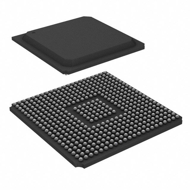
Virtex® Field Programmable Gate Array (FPGA) IC 316 81920 10800 432-LBGA Exposed Pad, Metal |
|---|---|
| Quantity | 939 Available (as of June 15, 2026) |

| Product Category | Field Programmable Gate Array (FPGA) |
|---|---|
| Manufacturer | AMD |
| Manufacturing Status | Obsolete |
| Manufacturer Standard Lead Time | Contact Us |
| Datasheet |
Specifications & Environmental
| Device Package | 432-MBGA (40x40) | Grade | Commercial | Operating Temperature | 0°C – 85°C | ||
|---|---|---|---|---|---|---|---|
| Package / Case | 432-LBGA Exposed Pad, Metal | Number of I/O | 316 | Voltage | 2.375 V - 2.625 V | ||
| Mounting Method | Surface Mount | RoHS Compliance | RoHS non-compliant | REACH Compliance | REACH Unaffected | ||
| Moisture Sensitivity Level | 3 (168 Hours) | Number of LABs/CLBs | 2400 | Number of Logic Elements/Cells | 10800 | ||
| Number of Gates | 468252 | ECCN | 3A991D | HTS Code | 8542.39.0001 | ||
| Qualification | N/A | Total RAM Bits | 81920 |
Overview of XCV400-4BG432C – Virtex® Field Programmable Gate Array (FPGA) IC, 316 I/O, 10,800 logic elements, ~0.082 Mbits RAM, 432-LBGA Exposed Pad
The XCV400-4BG432C is a Virtex® SRAM-based FPGA offering high-density programmable logic and a rich system feature set for commercial applications. Based on the Virtex architecture and built on a 0.22 µm, 5‑layer metal CMOS process, this device is optimized for designs that require a balance of logic capacity, I/O density, and embedded memory.
Typical market segments include compute and interface subsystems where reprogrammability, multi-standard I/O and advanced clock management enable rapid design iteration and system-level integration.
Key Features
- Logic Capacity — 10,800 logic elements (approximately 468,252 system gates) to implement complex combinatorial and sequential logic.
- Embedded Memory — Total on-chip RAM of 81,920 bits (approximately 0.082 Mbits) with LUTs configurable as various RAM and shift-register structures plus configurable 4k-bit dual-ported RAMs.
- I/O Density — 316 user I/Os supporting multi-standard SelectIO™ interfaces for diverse signaling requirements and direct connections to compatible memory devices.
- Clocking and Timing — Four dedicated delay-locked loops (DLLs), four primary low-skew global clock nets and 24 secondary local clock nets for flexible, low-jitter clock distribution.
- Arithmetic and Performance — Dedicated carry logic and multiplier support, cascade chains for wide-input functions, and register resources with clock enable and synchronous/asynchronous set/reset for high-speed datapaths; documented system performance up to 200 MHz and 66‑MHz PCI compliance.
- Configuration and Test — SRAM-based in-system configuration with four programming modes and IEEE 1149.1 boundary-scan support; 100% factory tested.
- Package and Mounting — Surface-mount 432-LBGA exposed pad, metal package (supplier device package: 432-MBGA, 40×40) suitable for compact board-level integration.
- Electrical and Environmental — VCC supply range 2.375 V to 2.625 V; commercial operating temperature range 0 °C to 85 °C; RoHS compliant.
Typical Applications
- High-speed interface bridging — Use the device’s multi-standard SelectIO™ and abundant I/O to implement protocol conversion, bus bridging, and custom interface logic.
- Data-path acceleration — Leverage dedicated carry and multiplier resources with deep register resources to implement arithmetic units, filters, and DSP front-ends.
- Memory controllers and buffering — Embedded RAM and configurable LUT-based RAM structures enable on-chip buffering and lightweight memory controllers for external memory interfaces.
- System glue and control logic — Implement control, sequencing, and glue logic between ASICs, CPUs, and peripherals, benefiting from reprogrammability during system development and field updates.
Unique Advantages
- Reprogrammable flexibility: SRAM-based configuration allows unlimited re-programmability and rapid design iteration without hardware respins.
- Balanced density and performance: Tens of thousands of gates and 10,800 logic elements provide a middle-ground solution for designs that need both capacity and timing headroom.
- Advanced clock management: Multiple DLLs and hierarchical clock networks simplify multi-clock domain designs and reduce clock skew across the fabric.
- Rich I/O capability: 316 I/Os and SelectIO™ compatibility support a wide range of external devices and signaling standards, reducing the need for external translators.
- Proven tool and ecosystem support: Supported by Xilinx Foundation™ and Alliance development systems and design flows for integration into existing toolchains.
Why Choose XCV400-4BG432C?
The XCV400-4BG432C combines a proven Virtex architecture with a practical mix of logic capacity, embedded memory and I/O density for commercial designs that require flexibility and in-field reprogrammability. Its built-in clock management, dedicated arithmetic resources and SelectIO™ interfaces help streamline implementation of complex data-paths and interface logic while maintaining a compact board footprint with the 432-LBGA exposed-pad package.
This device is well suited for engineering teams developing communication interfaces, custom accelerators, and system control logic who need a reliable, reprogrammable FPGA with comprehensive development support and verifiable electrical and thermal operating limits.
Request a quote or submit a purchase inquiry to receive availability and pricing information for the XCV400-4BG432C.


Date Founded: 1969
Headquarters: Santa Clara, California, USA
Employees: 25,000+
Revenue: $22.68 Billion
Certifications and Memberships: ISO9001:2015, RoHS, REACH


