
XCV400E-7PQ240C
| Part Description |
Virtex®-E Field Programmable Gate Array (FPGA) IC 158 163840 10800 240-BFQFP |
|---|---|
| Quantity | 136 Available (as of June 15, 2026) |

| Product Category | Field Programmable Gate Array (FPGA) |
|---|---|
| Manufacturer | AMD |
| Manufacturing Status | Obsolete |
| Manufacturer Standard Lead Time | Contact Us |
| Datasheet |
Specifications & Environmental
| Device Package | 240-PQFP (32x32) | Grade | Commercial | Operating Temperature | 0°C – 85°C | ||
|---|---|---|---|---|---|---|---|
| Package / Case | 240-BFQFP | Number of I/O | 158 | Voltage | 1.71 V - 1.89 V | ||
| Mounting Method | Surface Mount | RoHS Compliance | RoHS non-compliant | REACH Compliance | REACH Unaffected | ||
| Moisture Sensitivity Level | 3 (168 Hours) | Number of LABs/CLBs | 2400 | Number of Logic Elements/Cells | 10800 | ||
| Number of Gates | 569952 | ECCN | 3A001A7B | HTS Code | 8542.39.0001 | ||
| Qualification | N/A | Total RAM Bits | 163840 |
Overview of XCV400E-7PQ240C – Virtex®-E Field Programmable Gate Array (FPGA), 240-BFQFP
The XCV400E-7PQ240C is a Virtex®-E series Field Programmable Gate Array supplied in a 240-pin BFQFP surface-mount package. This commercial-grade, reprogrammable FPGA combines mid-range logic capacity with on-chip memory and flexible I/O to address embedded digital logic, interface bridging, and system prototyping applications.
Key device-level metrics include 10,800 logic elements, 569,952 gates, approximately 0.16 Mbits of embedded RAM, and 158 general-purpose I/Os. The device operates with an internal supply range of 1.71 V to 1.89 V and an ambient operating range of 0 °C to 85 °C.
Key Features
- Core logic 10,800 logic elements and 569,952 system gates provide the programmable fabric for combinational and sequential logic implementation.
- Embedded memory Approximately 163,840 bits of on-chip RAM give local data storage for FIFOs, buffers, and small lookup tables.
- I/O capacity and flexibility 158 I/Os allow extensive peripheral and bus interfacing; Virtex‑E series I/O architecture supports a wide range of signaling options and high‑performance interface standards.
- Clock management Built-in clock-management resources at the series level include multiple fully digital delay-locked loops (DLLs) to support flexible clocking and DDR-friendly timing.
- Performance characteristics Series-level performance characteristics include high internal operating frequency for multi-level LUT designs and support for high-speed source-synchronous interfaces.
- Power and supply Internal logic supply range of 1.71 V to 1.89 V; the family is designed for low-power operation as a series characteristic.
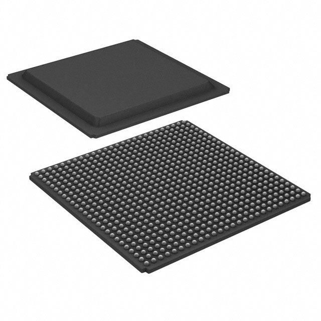
- Package and mounting 240-BFQFP surface-mount package (supplier device package: 240-PQFP, 32 × 32 mm) for straightforward PCB assembly.
- Operating grade and environmental Commercial grade device with an operating temperature range of 0 °C to 85 °C and RoHS compliance.
Typical Applications
- Communications & networking Use the device’s large I/O count and series-level support for high-performance interfaces to implement protocol bridging, packet processing, and interface conversion.
- Embedded system control Programmable logic and on-chip RAM make this FPGA well suited for custom control logic, sensor aggregation, and timing-critical embedded tasks.
- Memory interface and buffering On-chip RAM and configurable logic support local buffering, arbitration, and glue logic for external memory and bus subsystems.
- Prototyping and in-system reprogrammable designs Reprogrammability allows iterative hardware development, design validation, and field updates without changing hardware.
Unique Advantages
- Balanced logic and memory: 10,800 logic elements paired with approximately 0.16 Mbits of embedded RAM provide a versatile mix for control, datapath, and buffering tasks.
- Flexible I/O resources: 158 I/O pins give designers the ability to connect a broad set of peripherals and implement multi‑interface designs with fewer external components.
- Integrated clock resources: On-chip DLLs enable robust clocking strategies and DDR-friendly timing without extensive external clock conditioning.
- Commercial-grade reliability: Specified for 0 °C to 85 °C operation and RoHS compliant, suitable for a wide range of commercial and industrial-adjacent applications.
- Assembly-ready packaging: 240-BFQFP surface-mount package simplifies PCB assembly and prototyping workflows.
Why Choose XCV400E-7PQ240C?
The XCV400E-7PQ240C delivers a balanced FPGA option for designers who need substantial programmable logic, a moderate amount of embedded memory, and a high I/O count in a compact surface-mount package. Its commercial-grade rating and RoHS compliance make it appropriate for production embedded systems and development platforms where reprogrammability and interface flexibility are priorities.
This device is well suited to teams developing communication interfaces, custom controllers, or prototype systems that benefit from in-field reprogramming and a flexible logic/memory mix. The part’s electrical and thermal specifications provide clear, verifiable limits for system design and integration.
Request a quote or submit an inquiry to receive pricing and availability information for the XCV400E-7PQ240C.


Date Founded: 1969
Headquarters: Santa Clara, California, USA
Employees: 25,000+
Revenue: $22.68 Billion
Certifications and Memberships: ISO9001:2015, RoHS, REACH


