
XCV400E-8BG432C
| Part Description |
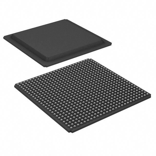
Virtex®-E Field Programmable Gate Array (FPGA) IC 316 163840 10800 432-LBGA Exposed Pad, Metal |
|---|---|
| Quantity | 236 Available (as of October 7, 2026) |

| Product Category | Field Programmable Gate Array (FPGA) |
|---|---|
| Manufacturer | AMD |
| Manufacturing Status | Obsolete |
| Manufacturer Standard Lead Time | Contact Us |
| Datasheet |
Specifications & Environmental
| Device Package | 432-MBGA (40x40) | Grade | Commercial | Operating Temperature | 0°C – 85°C | ||
|---|---|---|---|---|---|---|---|
| Package / Case | 432-LBGA Exposed Pad, Metal | Number of I/O | 316 | Voltage | 1.71 V - 1.89 V | ||
| Mounting Method | Surface Mount | RoHS Compliance | RoHS non-compliant | REACH Compliance | REACH Unaffected | ||
| Moisture Sensitivity Level | 3 (168 Hours) | Number of LABs/CLBs | 2400 | Number of Logic Elements/Cells | 10800 | ||
| Number of Gates | 569952 | ECCN | 3A991D | HTS Code | 8542.39.0001 | ||
| Qualification | N/A | Total RAM Bits | 163840 |
Overview of XCV400E-8BG432C – Virtex®-E Field Programmable Gate Array (FPGA)
The XCV400E-8BG432C is a Virtex®-E family FPGA in a 432-pin LBGA package designed for commercial embedded and system applications. It implements the 1.8 V Virtex‑E architecture and provides a combination of on-chip logic, embedded memory, and high I/O count for custom digital functions and interface logic.
With 10,800 logic elements, approximately 0.16 Mbits of embedded memory, and 316 available I/O, this device is suited to designs that require flexible programmable logic, substantial I/O bandwidth, and in-system reprogrammability.
Key Features
- Core Architecture Virtex‑E 1.8 V FPGA family architecture with documented family-level capabilities and support for SRAM-based in-system configuration.
- Logic Resources 10,800 logic elements and 569,952 gates for implementing complex custom logic and state machines.
- Embedded Memory Total on-chip RAM of 163,840 bits (approximately 0.16 Mbits) for buffering, FIFOs, and small embedded data stores.
- I/O Density and Standards 316 I/O pins provided in the 432-LBGA package; family-level SelectI/O+ features support multiple high-performance interface standards and differential signalling options.
- Performance Family documentation cites internal performance up to 130 MHz (four LUT levels) and support for high-speed clock inputs for demanding timing requirements.
- Clock Management Family-level clock management includes multiple digital DLLs for clock multiplication, division, and duty-cycle control.
- Package and Mounting 432-LBGA exposed pad, metal package (supplier device package: 432-MBGA 40×40); surface-mount mounting type.
- Power and Operating Range Core supply range 1.71 V to 1.89 V; commercial grade operating temperature 0 °C to 85 °C.
- Compliance RoHS compliant.
Typical Applications
- High-speed interface controllers — Implement PCI and other bus interfaces or custom interface logic that benefit from dense I/O and programmable timing.
- Memory interface and buffering — Use on-chip RAM and logic to build memory controllers, FIFOs, and data-path buffering for system designs.
- Custom digital processing — Offload application-specific processing and control functions into reprogrammable logic to reduce system BOM.
- Multi-standard I/O bridging — Implement protocol conversion and signal conditioning leveraging the device’s extensive I/O resources and differential signalling support.
Unique Advantages
- Substantial programmable logic: 10,800 logic elements provide the capacity to implement complex glue logic, custom accelerators, and control functions.
- Significant on-chip memory: Approximately 0.16 Mbits of embedded RAM enables localized buffering and reduces external memory dependence for many functions.
- High I/O count in a compact package: 316 I/Os in a 432-LBGA (40×40) package supports dense multi-channel interfaces while conserving board area.
- Family-level clock and interface features: Documented Virtex‑E capabilities for DLL-based clock management and support for high-performance I/O standards facilitate robust timing and interface design.
- Commercial temperature and RoHS compliance: Designed for 0 °C to 85 °C operation and RoHS-compliant manufacturing to meet common commercial program requirements.
Why Choose XCV400E-8BG432C?
The XCV400E-8BG432C combines a Virtex‑E FPGA architecture with a balanced set of logic, memory, and I/O resources for designs that require flexible, reprogrammable hardware. Its 10,800 logic elements, substantial I/O count, and embedded RAM make it well suited to system-level functions such as interface controllers, memory buffering, and custom digital processing.
Supported by the Virtex‑E family feature set and development ecosystem, this device offers designers a reprogrammable platform that scales from prototype to production in commercial environments, enabling iterative development and in-system updates.
Request a quote or submit a purchase inquiry for the XCV400E-8BG432C to receive pricing and availability information for your next design.





















Date Founded: 1969
Headquarters: Santa Clara, California, USA
Employees: 25,000+
Revenue: $22.68 Billion
Certifications and Memberships: ISO9001:2015, RoHS, REACH











