
XCV405E-8FG676C
| Part Description |
Virtex®-E EM Field Programmable Gate Array (FPGA) IC 404 573440 10800 676-BGA |
|---|---|
| Quantity | 1,188 Available (as of June 15, 2026) |

| Product Category | Field Programmable Gate Array (FPGA) |
|---|---|
| Manufacturer | AMD |
| Manufacturing Status | Obsolete |
| Manufacturer Standard Lead Time | Contact Us |
| Datasheet |
Specifications & Environmental
| Device Package | 676-FBGA (27x27) | Grade | Commercial | Operating Temperature | 0°C – 85°C | ||
|---|---|---|---|---|---|---|---|
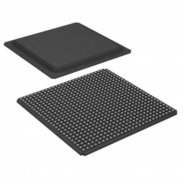
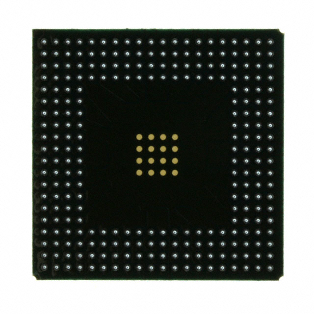
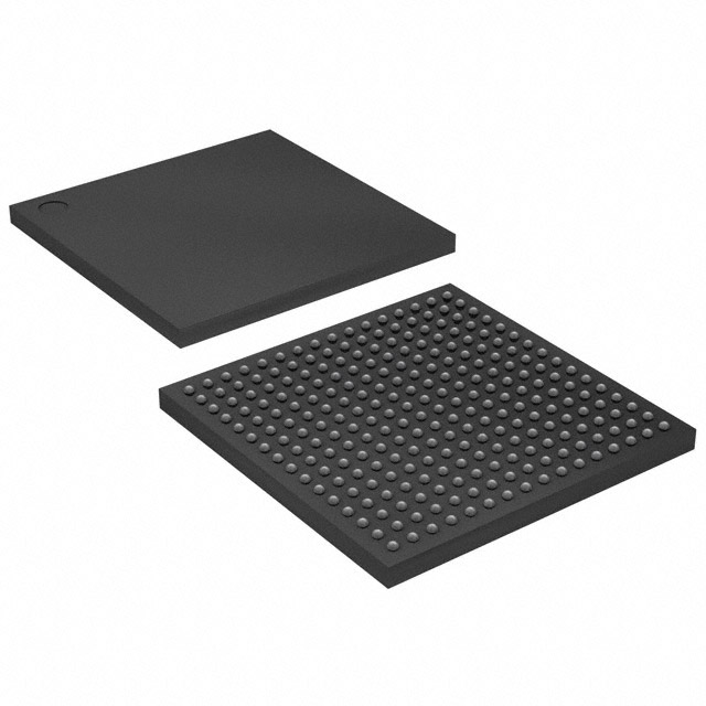
| Package / Case | 676-BGA | Number of I/O | 404 | Voltage | 1.71 V - 1.89 V | ||
| Mounting Method | Surface Mount | RoHS Compliance | RoHS non-compliant | REACH Compliance | REACH Unaffected | ||
| Moisture Sensitivity Level | 3 (168 Hours) | Number of LABs/CLBs | 2400 | Number of Logic Elements/Cells | 10800 | ||
| Number of Gates | 129600 | ECCN | 3A991D | HTS Code | 8542.39.0001 | ||
| Qualification | N/A | Total RAM Bits | 573440 |
Overview of XCV405E-8FG676C – Virtex®-E EM Field Programmable Gate Array (FPGA) IC 404 573440 10800 676-BGA
The XCV405E-8FG676C is a Virtex®-E EM Field Programmable Gate Array (FPGA) from AMD, delivered in a 676-FBGA (27×27) surface-mount package. It integrates 2,400 CLBs and 10,800 logic elements with approximately 0.57 Mbits of embedded memory and a 404-pin I/O count, providing on-chip resources for complex logic and I/O interfacing.
Designed for commercial-grade applications, this FPGA operates from a 1.71 V to 1.89 V core supply and supports an ambient temperature range of 0 °C to 85 °C. It is RoHS compliant and packaged for high-density board designs requiring a 676-BGA footprint.
Key Features
- Core Logic 2,400 CLBs and 10,800 logic elements enable implementation of complex programmable logic functions.
- Embedded Memory Approximately 0.57 Mbits of on-chip RAM (573,440 bits) for storage and buffering within logic designs.
- I/O Capacity 404 user I/O pins to support extensive interfacing and signaling requirements.
- Gate Density 129,600 gates to accommodate moderately complex gate-level implementations and glue logic.
- Package & Mounting 676-BGA (supplier device package: 676-FBGA, 27×27) surface-mount package for high pin-count, compact board layouts.
- Power Core voltage range of 1.71 V to 1.89 V to match system power-rail requirements.
- Operating Conditions & Compliance Commercial operating temperature 0 °C to 85 °C and RoHS compliant.
Typical Applications
- FPGA Prototyping and Development Use the device’s 10,800 logic elements and 2,400 CLBs for hardware prototyping and validation of custom logic designs.
- High-Density I/O Systems The 404 I/O pins support designs that require extensive external interfacing or parallel signal routing.
- Embedded Memory-Dependent Designs Approximately 0.57 Mbits of on-chip RAM can be applied for buffering, small data tables, or state storage within logic fabrics.
- Compact Board Implementations The 676-FBGA package is suitable for space-constrained PCBs that need a high pin count in a compact footprint.
Unique Advantages
- Substantial Logic Capacity: 10,800 logic elements and 2,400 CLBs provide the resources needed for medium-to-complex logic implementations without external ASICs.
- Meaningful On-Chip Memory: Approximately 0.57 Mbits of embedded RAM reduces dependence on external memory for many control and buffering tasks.
- Large I/O Complement: 404 available I/O pins support extensive peripheral and signaling connectivity directly from the FPGA.
- High Gate Count: 129,600 gates offer the density required for integrating multiple functions on a single device.
- Compact, High-Pin-Count Package: 676-FBGA (27×27) supports high-density board layouts while maintaining a surface-mount form factor.
- Commercial-Grade and RoHS Compliant: Specified 0 °C to 85 °C operation and RoHS compliance fit standard commercial electronic designs and regulatory needs.
Why Choose XCV405E-8FG676C?
The XCV405E-8FG676C positions itself as a commercially graded Virtex®-E FPGA that combines moderate to high logic capacity, significant embedded memory, and a large I/O count in a compact 676-BGA package. Its specification set—2,400 CLBs, 10,800 logic elements, 404 I/O, and approximately 0.57 Mbits of on-chip RAM—makes it suitable for designers seeking to consolidate multiple functions into a single programmable device while maintaining a commercial temperature profile.
This part is well suited to teams developing board-level systems that require a balance of logic density, embedded memory, and high pin-count connectivity in a surface-mount FBGA package from AMD.
Request a quote or submit an inquiry to obtain pricing, availability, and additional purchase information for XCV405E-8FG676C.


Date Founded: 1969
Headquarters: Santa Clara, California, USA
Employees: 25,000+
Revenue: $22.68 Billion
Certifications and Memberships: ISO9001:2015, RoHS, REACH


