
XCV50-4FG256C
| Part Description |
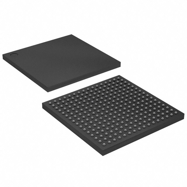
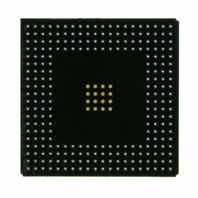
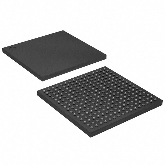
Virtex® Field Programmable Gate Array (FPGA) IC 176 32768 1728 256-BGA |
|---|---|
| Quantity | 970 Available (as of October 8, 2026) |
| Product Category | Field Programmable Gate Array (FPGA) |
|---|---|
| Manufacturer | AMD |
| Manufacturing Status | Obsolete |
| Manufacturer Standard Lead Time | Contact Us |
| Datasheet |
Specifications & Environmental
| Device Package | 256-FBGA (17x17) | Grade | Commercial | Operating Temperature | 0°C – 85°C | ||
|---|---|---|---|---|---|---|---|
| Package / Case | 256-BGA | Number of I/O | 176 | Voltage | 2.375 V - 2.625 V | ||
| Mounting Method | Surface Mount | RoHS Compliance | RoHS non-compliant | REACH Compliance | REACH Unaffected | ||
| Moisture Sensitivity Level | 3 (168 Hours) | Number of LABs/CLBs | 384 | Number of Logic Elements/Cells | 1728 | ||
| Number of Gates | 57906 | ECCN | EAR99 | HTS Code | 8542.39.0001 | ||
| Qualification | N/A | Total RAM Bits | 32768 |
Overview of XCV50-4FG256C – Virtex® Field Programmable Gate Array (FPGA) IC 176 32768 1728 256-BGA
The XCV50-4FG256C is an SRAM-based Virtex FPGA offering 57,906 system gates in a 256-ball BGA package. Its architecture combines a regular array of configurable logic with abundant routing, on-chip memory, and multi-standard I/O to address programmable-logic requirements in communications, embedded systems, prototyping, and board-level I/O bridging.
This device delivers a balance of logic capacity and I/O density with 1,728 logic elements, 32,768 bits of embedded RAM, and 176 I/O pins, alongside built-in clock-management and in-system configuration features for flexible design integration and re-programmability.
Key Features
- Core Architecture 1,728 logic elements and 57,906 system gates in a regular CLB array optimized for place-and-route efficiency.
- On-Chip Memory 32,768 bits of embedded RAM to support LUT-based RAM and dual-ported RAM configurations.
- I/O Density 176 user I/O pins provide flexible board-level interfacing and high pin-count connectivity.
- Clock Management Four dedicated delay-locked loops (DLLs), four primary low-skew global clock nets and 24 secondary local clock nets for advanced clock control and distribution.
- Arithmetic and Logic Support Dedicated carry logic and multiplier support for efficient implementation of high-speed arithmetic functions.
- Configuration and Re-programmability SRAM-based in-system configuration with unlimited re-programmability and four programming modes for iterative development and field updates.
- Package and Mounting 256-ball BGA (256-FBGA, 17×17) surface-mount package suitable for compact, high-density board designs.
- Electrical and Temperature Supply voltage range 2.375 V to 2.625 V and commercial operating temperature range 0 °C to 85 °C.
- Manufacturing and Quality 100% factory tested as part of the Virtex family manufacturing flow.
Typical Applications
- PCI and Board-Level I/O Bridging — Leveraging the device’s multi-standard SelectIO interfaces and series support for 66-MHz PCI compliance and hot-swap applications to implement board-level bridging and legacy interface support.
- Embedded System Prototyping — Use the FPGA’s re-programmability and on-chip RAM to iterate system logic quickly during development and verification.
- High-Density Logic Integration — Implement medium-complexity state machines, control logic, and custom peripherals using 1,728 logic elements and dedicated arithmetic resources.
- Memory Interface and Acceleration — Integrate fast interfaces to external high-performance RAM and use embedded RAM blocks for buffering and local data storage.
Unique Advantages
- Balanced Logic and I/O in a Compact Package: 1,728 logic elements with 176 I/O pins in a 256-ball BGA enable dense functionality in space-constrained designs.
- Flexible Clocking: Four DLLs and multiple global/local clock nets simplify complex clock-tree designs and timing control.
- On-Device Memory: 32,768 bits of embedded RAM reduce dependence on external memory for many buffering and small-data storage needs.
- Re-programmable Development Flow: SRAM-based configuration with unlimited re-programmability and four programming modes supports rapid design iteration and in-system updates.
- Proven Manufacturing Quality: 100% factory-tested device within the Virtex family provides traceable production quality.
Why Choose XCV50-4FG256C?
The XCV50-4FG256C positions itself as a commercially graded Virtex FPGA that combines a well-balanced set of logic resources, embedded memory, and high I/O count in a compact 256-FBGA package. Its on-chip clock-management features, dedicated arithmetic support, and SRAM-based in-system configuration make it well suited for designs that require flexible, re-programmable logic with reliable board-level interfacing.
This device is suitable for engineering teams and procurement looking for a tested, commercially graded FPGA with established series-level features and development ecosystem support for medium-complexity programmable logic tasks.
Request a quote or submit an RFQ to receive pricing and availability for the XCV50-4FG256C.





















Date Founded: 1969
Headquarters: Santa Clara, California, USA
Employees: 25,000+
Revenue: $22.68 Billion
Certifications and Memberships: ISO9001:2015, RoHS, REACH











