
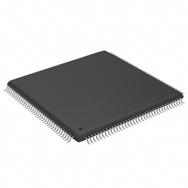
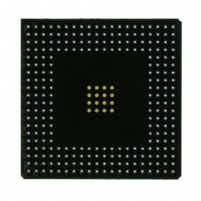
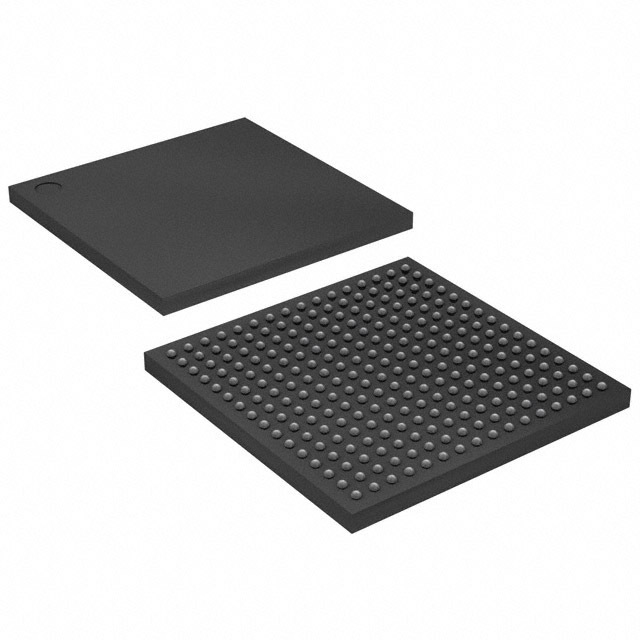
XCV50-4PQ240C
| Part Description |
Virtex® Field Programmable Gate Array (FPGA) IC 166 32768 1728 240-BFQFP |
|---|---|
| Quantity | 536 Available (as of June 15, 2026) |

| Product Category | Field Programmable Gate Array (FPGA) |
|---|---|
| Manufacturer | AMD |
| Manufacturing Status | Obsolete |
| Manufacturer Standard Lead Time | Contact Us |
| Datasheet |
Specifications & Environmental
| Device Package | 240-PQFP (32x32) | Grade | Commercial | Operating Temperature | 0°C – 85°C | ||
|---|---|---|---|---|---|---|---|
| Package / Case | 240-BFQFP | Number of I/O | 166 | Voltage | 2.375 V - 2.625 V | ||
| Mounting Method | Surface Mount | RoHS Compliance | RoHS non-compliant | REACH Compliance | REACH Unaffected | ||
| Moisture Sensitivity Level | 3 (168 Hours) | Number of LABs/CLBs | 384 | Number of Logic Elements/Cells | 1728 | ||
| Number of Gates | 57906 | ECCN | EAR99 | HTS Code | 8542.39.0001 | ||
| Qualification | N/A | Total RAM Bits | 32768 |
Overview of XCV50-4PQ240C – Virtex® Field Programmable Gate Array (FPGA) IC 166 32768 1728 240-BFQFP
The XCV50-4PQ240C is a Virtex-series SRAM-based FPGA offering a balance of logic capacity, embedded memory, and flexible I/O in a 240-pin BFQFP surface-mount package. With 1,728 logic elements and approximately 32,768 bits of on-chip RAM, this device targets embedded and system designs that require reprogrammable logic, configurable memory, and multi-standard I/O capability.
Typical use cases include system prototyping, compact PCI/PCI interface implementations, and applications that benefit from dedicated clock management and arithmetic support. The device provides a combination of configurable logic, hierarchical memory, and on-chip clock resources to simplify system-level integration.
Key Features
- Logic Capacity — 1,728 logic elements and 384 CLBs provide a compact array for implementing custom logic and control functions.
- Embedded Memory — 32,768 bits of block RAM organized in a hierarchical memory system; LUTs can be configured as various small RAM structures or shift registers to support on-chip data buffering and state storage.
- I/O — 166 user I/O pins support multi-standard SelectIO interfaces and facilitate connections to a wide range of external devices and memories.
- Clock Management — Four dedicated delay-locked loops (DLLs), four primary low-skew global clock nets, and 24 secondary local clock nets enable advanced clock control and distribution for synchronous designs.
- Arithmetic and DSP Support — Dedicated carry logic and multiplier support accelerate high-speed arithmetic functions and signal processing tasks.
- Configuration and Re-programmability — SRAM-based in-system configuration with unlimited re-programmability and four programming modes provides flexible development and field update options.
- Package and Mounting — 240-BFQFP (supplier package: 240-PQFP, 32×32) in a surface-mount form factor suited for compact PCB designs.
- Electrical and Temperature — Core supply voltage range 2.375 V to 2.625 V; commercial-grade operating temperature range 0 °C to 85 °C.
- Process and Test — 0.22 µm, 5-layer metal CMOS process and 100% factory tested for production-level quality control.
- Compliance — RoHS compliant.
Typical Applications
- PCI and Compact PCI Interfaces — Implements 66-MHz PCI-compliant logic and supports hot-swapping for Compact PCI systems where reconfigurable logic is required.
- Embedded System Control — Ideal for control logic, protocol bridging, and peripheral interfacing in embedded platforms thanks to flexible I/O and on-chip RAM.
- Signal Processing and Arithmetic Acceleration — Dedicated multiplier and carry logic accelerate arithmetic-heavy blocks such as filters or custom DSP functions.
- Prototyping and In-System Upgrades — SRAM-based configuration and unlimited re-programmability support iterative development and field updates without board respins.
Unique Advantages
- Balanced integration of logic and memory — 1,728 logic elements paired with 32,768 bits of block RAM enables compact implementations of control and data paths on a single device.
- Advanced clocking resources — Multiple DLLs and hierarchical clock nets simplify timing management across complex synchronous designs.
- Flexible I/O support — Multi-standard SelectIO capability and 166 user I/Os make it straightforward to interface with diverse external components and memories.
- Re-programmable development flow — SRAM-based architecture with multiple programming modes supports rapid prototyping and field reconfiguration.
- Commercial temperature and compact package — Surface-mount 240-BFQFP package and 0 °C to 85 °C rating suit a range of commercial electronic products.
- Manufacturing reliability — Fabricated on a 0.22 µm, 5-layer metal process and 100% factory tested for production consistency.
Why Choose XCV50-4PQ240C?
The XCV50-4PQ240C delivers a practical combination of reprogrammable logic, on-chip memory, and deterministic clock resources for designers needing a compact, flexible FPGA solution. It is well suited to teams implementing PCI/Compact PCI interfaces, embedded control systems, or arithmetic-accelerated blocks that benefit from dedicated multipliers and carry logic.
With a commercial temperature rating, surface-mount 240-pin package, and RoHS compliance, the device provides a production-ready building block that supports development agility through in-system re-programmability and proven manufacturing test coverage.
Request a quote or submit an inquiry to receive pricing and availability for the XCV50-4PQ240C and to discuss how this FPGA can fit your next design.


Date Founded: 1969
Headquarters: Santa Clara, California, USA
Employees: 25,000+
Revenue: $22.68 Billion
Certifications and Memberships: ISO9001:2015, RoHS, REACH


