
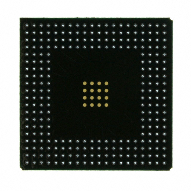
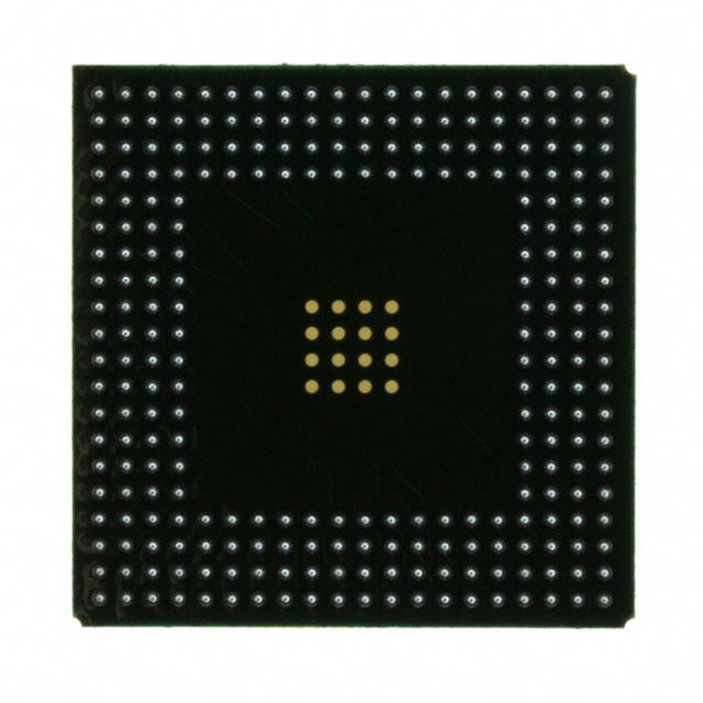
XCV50-4BG256C
| Part Description |
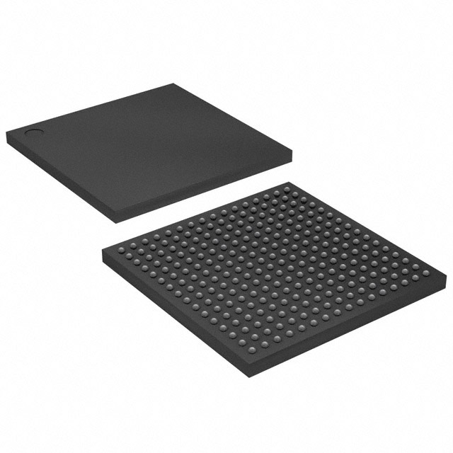
Virtex® Field Programmable Gate Array (FPGA) IC 180 32768 1728 256-BBGA |
|---|---|
| Quantity | 27 Available (as of October 7, 2026) |
| Product Category | Field Programmable Gate Array (FPGA) |
|---|---|
| Manufacturer | AMD |
| Manufacturing Status | Obsolete |
| Manufacturer Standard Lead Time | Contact Us |
| Datasheet |
Specifications & Environmental
| Device Package | 256-PBGA (27x27) | Grade | Commercial | Operating Temperature | 0°C – 85°C | ||
|---|---|---|---|---|---|---|---|
| Package / Case | 256-BBGA | Number of I/O | 180 | Voltage | 2.375 V - 2.625 V | ||
| Mounting Method | Surface Mount | RoHS Compliance | RoHS non-compliant | REACH Compliance | REACH Unaffected | ||
| Moisture Sensitivity Level | 3 (168 Hours) | Number of LABs/CLBs | 384 | Number of Logic Elements/Cells | 1728 | ||
| Number of Gates | 57906 | ECCN | EAR99 | HTS Code | 8542.39.0001 | ||
| Qualification | N/A | Total RAM Bits | 32768 |
Overview of XCV50-4BG256C – Virtex Field Programmable Gate Array, 256-BBGA
The XCV50-4BG256C is an SRAM-based Virtex FPGA offering a balanced mix of logic capacity, on-chip memory and I/O density in a 256-ball BGA package. Built on the Virtex architecture, the device exposes approximately 1,728 logic elements, 32,768 bits of on-chip RAM and 180 user I/O pins, targeting commercial designs that require reprogrammable, high‑performance programmable logic.
Designed for applications that require flexible clocking, multi-standard interfaces and in-system reconfiguration, this Virtex device combines core FPGA features — including dedicated clock-management, configurable LUT-based memory and abundant registers — with a 2.375 V–2.625 V supply window and a 0 °C to 85 °C operating range.
Key Features
- Logic Capacity — Approximately 1,728 logic elements and around 57,906 system gates provide mid-range programmable logic resources for glue logic, protocol handling and custom datapaths.
- Embedded Memory — 32,768 bits of on-chip RAM support block- and LUT-based memory structures for FIFOs, buffers and small on-chip storage.
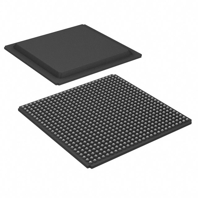
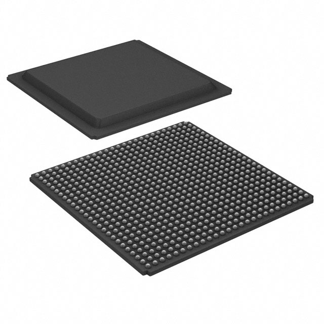
- I/O Density & Interfaces — 180 user I/O pins in a 256-BBGA (256-PBGA, 27 × 27 mm) package enable dense board-level connectivity for parallel buses, peripheral interfaces and system I/O.
- Clocking & Timing — Built-in clock-management features (including multiple delay-locked loops and dedicated global clock nets as described in the Virtex family specification) support advanced clock control and low-skew distribution.
- Configuration & Reprogrammability — SRAM-based in-system configuration allows unlimited re-programmability and multiple programming modes for field updates and development iterations.
- Power & Supply — Operates from a core supply range of 2.375 V to 2.625 V, suitable for designs matching the Virtex 2.5 V family supply requirements.
- Package & Mounting — Surface-mount 256-BBGA package (256-PBGA, 27 × 27 mm) supports compact board integration and high pin-count designs.
- Commercial Temperature Grade — Rated for operation from 0 °C to 85 °C for commercial applications; RoHS compliant.
Typical Applications
- Communications & Networking — Implement protocol translation, interface bridging or custom packet-processing logic using the device’s I/O density and reprogrammable logic.
- PCI and CompactPCI Systems — Suitable for designs that leverage the Virtex family’s support for PCI-compliant implementations and hot‑swappable CompactPCI architectures as described in the family specification.
- Embedded Systems & Prototyping — Reprogrammability and on-chip memory make the device useful for iterative hardware development, algorithm prototyping and embedded controller functions.
- Instrumentation & Test Equipment — Use the FPGA for data capture, pre‑processing and custom timing control where flexible logic and deterministic I/O are required.
Unique Advantages
- Balanced Logic and Memory — The combination of approximately 1,728 logic elements and 32,768 bits of on-chip RAM supports mid-density designs without external memory for many control and buffering tasks.
- High I/O Count in Compact Package — 180 user I/O pins in a 27 × 27 mm 256-BBGA deliver significant connectivity while conserving board area.
- Reprogrammable SRAM Architecture — In-system configurability enables field updates and iterative development flows, reducing time-to-market for evolving designs.
- Advanced Clock Management — Dedicated DLLs and hierarchical clock resources (as provided by the Virtex family) simplify multi-clock-domain designs and reduce clock skew concerns.
- Commercial-Grade Reliability — Specified for 0 °C to 85 °C operation and RoHS compliant for standard commercial deployment.
Why Choose XCV50-4BG256C?
The XCV50-4BG256C positions itself as a practical Virtex-class FPGA for commercial designs that need reprogrammable logic, moderate gate density and substantial I/O capability in a compact BGA package. Its combination of logic elements, embedded RAM and clocking resources supports a range of mid-density applications from communications interfaces to embedded control and test equipment.
For developers and procurement teams seeking a field-updatable, RoHS-compliant FPGA with a clear supply voltage and temperature specification, the XCV50-4BG256C offers a dependable platform consistent with the Virtex family’s architecture and toolchain support.
Request a quote or submit an RFQ to receive pricing, availability and lead-time information for the XCV50-4BG256C. Our team can provide technical details and support to help evaluate integration into your design.





















Date Founded: 1969
Headquarters: Santa Clara, California, USA
Employees: 25,000+
Revenue: $22.68 Billion
Certifications and Memberships: ISO9001:2015, RoHS, REACH











