
XCV50E-6PQ240I
| Part Description |
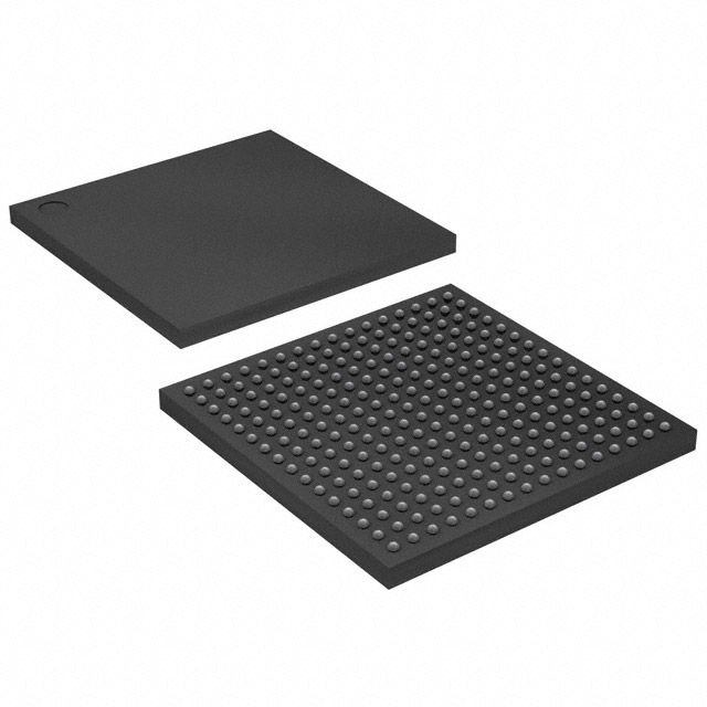
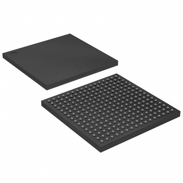
Virtex®-E Field Programmable Gate Array (FPGA) IC 158 65536 1728 240-BFQFP |
|---|---|
| Quantity | 599 Available (as of October 8, 2026) |

| Product Category | Field Programmable Gate Array (FPGA) |
|---|---|
| Manufacturer | AMD |
| Manufacturing Status | Obsolete |
| Manufacturer Standard Lead Time | Contact Us |
| Datasheet |
Specifications & Environmental
| Device Package | 240-PQFP (32x32) | Grade | Industrial | Operating Temperature | -40°C – 100°C | ||
|---|---|---|---|---|---|---|---|
| Package / Case | 240-BFQFP | Number of I/O | 158 | Voltage | 1.71 V - 1.89 V | ||
| Mounting Method | Surface Mount | RoHS Compliance | RoHS non-compliant | REACH Compliance | REACH Unaffected | ||
| Moisture Sensitivity Level | 3 (168 Hours) | Number of LABs/CLBs | 384 | Number of Logic Elements/Cells | 1728 | ||
| Number of Gates | 71693 | ECCN | EAR99 | HTS Code | 8542.39.0001 | ||
| Qualification | N/A | Total RAM Bits | 65536 |
Overview of XCV50E-6PQ240I – Virtex®-E Field Programmable Gate Array (FPGA) IC 158 65536 1728 240-BFQFP
The XCV50E-6PQ240I is an AMD Virtex®-E series FPGA supplied in a 240-BFQFP surface-mount package. It combines a compact logic array with on-chip RAM and flexible I/O to support custom digital designs for industrial applications.
Key architectural attributes include 384 logic blocks providing 1,728 logic elements, approximately 65,536 bits (≈0.06 Mbits) of embedded RAM, 158 user I/O pins, and an internal core voltage range of 1.71 V to 1.89 V. The device is rated for industrial operating temperatures from −40 °C to 100 °C and is designed for low-power operation with SRAM-based in-system reprogrammability.
Key Features
- Core Architecture 384 logic blocks delivering 1,728 logic elements and an equivalent of 71,693 gates for implementing custom logic functions.
- Embedded Memory Approximately 65,536 bits (≈0.06 Mbits) of on-chip RAM for distributed storage and small buffering tasks.
- I/O Flexibility 158 user I/Os; SelectI/O+ technology supports a wide range of interface standards and differential signaling (LVDS, BLVDS, LVPECL) for high-speed serial or parallel links.
- Clocking and Timing Includes advanced clock management features from the Virtex‑E family such as fully digital delay-locked loops (DLLs) for clock multiply/divide and precise phase control.
- Power and Voltage 1.8 V core operation with a specified supply range of 1.71 V to 1.89 V, designed for low-power operation on the Virtex‑E process.
- Package and Mounting 240-BFQFP (240-PQFP, 32 × 32 mm footprint) surface-mount package suitable for compact board designs.
- Industrial Temperature Grade Specified operating temperature range of −40 °C to 100 °C for deployment in industrial environments.
- In-System Reconfiguration SRAM-based in-system configuration enables unlimited reprogramming for iterative development and field updates.
Typical Applications
- High-performance memory interfaces Use for interfacing to external memories such as DDR SDRAM and ZBT SRAM where flexible logic and timing control are required.
- PCI and bus bridging Suitable for 3.3 V PCI-compliant system designs that require configurable logic for bus bridging and protocol adaptation.
- High-speed serial interfaces Differential signaling support (LVDS, BLVDS, LVPECL) enables implementation of low-skew, high-bandwidth links and serializer/deserializer functions.
- Industrial control and automation Industrial temperature rating and reprogrammability make the device well suited for PLCs, motion control, and other factory automation tasks that benefit from field updates and custom logic.
Unique Advantages
- Reprogrammable platform: SRAM-based in-system configuration allows design iteration and firmware updates without hardware changes.
- Flexible I/O standards: SelectI/O+ and differential signaling support provide broad compatibility with modern interface requirements, reducing external translator components.
- Integrated clock management: Digital DLLs and clock synthesis capabilities simplify timing design for high-speed and DDR applications.
- Industrial-ready packaging and thermal range: 240-BFQFP surface-mount package combined with −40 °C to 100 °C rating supports robust deployment in industrial environments.
- Compact memory and logic mix: On-chip RAM and 1,728 logic elements offer a balanced platform for control, buffering, and mid-range logic integration.
Why Choose XCV50E-6PQ240I?
The XCV50E-6PQ240I brings a balanced combination of configurable logic, embedded memory, and flexible I/O in a rugged industrial-grade package. Its 1.8 V core operation, wide I/O capability, and SRAM-based reprogramming fit designs that require field-updatable logic, precision clocking, and support for high-speed differential interfaces.
This device is well suited for engineers developing industrial communications, memory interface controllers, PCI-based subsystems, and other mid-density FPGA applications that demand a reliable, reconfigurable solution backed by Virtex‑E family development tools and ecosystem support.
Request a quote or submit an RFQ for XCV50E-6PQ240I today to evaluate fit for your next design.






















Date Founded: 1969
Headquarters: Santa Clara, California, USA
Employees: 25,000+
Revenue: $22.68 Billion
Certifications and Memberships: ISO9001:2015, RoHS, REACH











