
XCV50E-7CS144C
| Part Description |
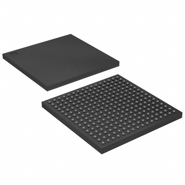
Virtex®-E Field Programmable Gate Array (FPGA) IC 94 65536 1728 144-TFBGA, CSPBGA |
|---|---|
| Quantity | 444 Available (as of June 15, 2026) |

| Product Category | Field Programmable Gate Array (FPGA) |
|---|---|
| Manufacturer | AMD |
| Manufacturing Status | Obsolete |
| Manufacturer Standard Lead Time | Contact Us |
| Datasheet |
Specifications & Environmental
| Device Package | 144-LCSBGA (12x12) | Grade | Commercial | Operating Temperature | 0°C – 85°C | ||
|---|---|---|---|---|---|---|---|
| Package / Case | 144-TFBGA, CSPBGA | Number of I/O | 94 | Voltage | 1.71 V - 1.89 V | ||
| Mounting Method | Surface Mount | RoHS Compliance | RoHS non-compliant | REACH Compliance | REACH Unaffected | ||
| Moisture Sensitivity Level | 3 (168 Hours) | Number of LABs/CLBs | 384 | Number of Logic Elements/Cells | 1728 | ||
| Number of Gates | 71693 | ECCN | EAR99 | HTS Code | 8542.39.0001 | ||
| Qualification | N/A | Total RAM Bits | 65536 |
Overview of XCV50E-7CS144C – Virtex®-E FPGA, 1,728 logic elements, 64 Kbit RAM, 94 I/Os, 144‑TFBGA
The XCV50E-7CS144C is a Virtex®-E series Field Programmable Gate Array (FPGA) supplied in a 144‑TFBGA/CSPBGA package for surface-mount applications. Built on the Virtex‑E 1.8 V FPGA architecture, it targets commercial embedded designs that require reprogrammable logic, flexible I/O connectivity and on-chip RAM for control, glue-logic and interface tasks.
With 1,728 logic elements, 65,536 bits of on-chip RAM and 94 user I/O pins, this device is optimized for mid-density FPGA roles where moderate logic capacity, configurable memory and a compact package are key design considerations.
Key Features
- Core Architecture — Virtex‑E 1.8 V FPGA family architecture providing programmable logic and system integration capability.
- Logic Resources — 1,728 logic elements (reported) and approximately 71,693 gates for mid-density designs and control/processing functions.
- Embedded Memory — 65,536 total RAM bits (approximately 64 Kbits) of on-chip memory for buffering, FIFOs and small data structures.
- I/O Count & Flexibility — 94 user I/Os to support multiple interfaces and peripheral connections in a compact footprint.
- Voltage & Power — Core operating supply 1.71 V to 1.89 V as specified for the device.
- Package & Mounting — 144‑TFBGA (CSPBGA) surface-mount package; supplier device package listed as 144‑LCSBGA (12×12).
- Operating Range — Commercial grade with an operating temperature range of 0 °C to 85 °C.
- RoHS Compliance — Device is RoHS compliant.
- Family-Level Capabilities — Based on the Virtex‑E family which includes features such as SelectI/O+ differential signalling support, built-in clock management (DLLs) and SRAM-based in-system configuration (family-level information).
Typical Applications
- Embedded Control and Glue Logic — Use the on-chip logic and RAM for application-specific control paths, protocol adaptation and peripheral interfacing in commercial embedded systems.
- Interface Handling — With 94 I/Os, implement multi-signal interface bridging, custom bus adapters or front-end I/O aggregation for communications or instrumentation equipment.
- Memory Interface Support — Implement local buffering, small FIFOs and timing adaptation when interfacing to external memory or peripherals.
- Prototyping and Development — Reprogrammable SRAM-based configuration enables iterative design and firmware updates during system bring-up and evaluation.
Unique Advantages
- Balanced Resource Set: Combines 1,728 logic elements with 64 Kbits of embedded RAM to address moderate-density logic and memory needs without excessive board area.
- Flexible I/O Count: Ninety-four I/Os provide versatility for multi-signal designs, reducing the need for additional interface ICs.
- Compact Surface-Mount Package: 144‑TFBGA/CSPBGA footprint enables space-efficient board layout for compact commercial products.
- Commercial Temperature Rating: Rated 0 °C to 85 °C to match typical commercial embedded product environments.
- Standards-Aligned Family Features: Leverages Virtex‑E family capabilities (such as SelectI/O+ and DLL-based clock management) for easier integration into systems that require robust clock and I/O handling (family-level reference).
- RoHS Compliant: Meets RoHS requirements for lead-free assembly and regulatory conformity in commercial markets.
Why Choose XCV50E-7CS144C?
The XCV50E-7CS144C delivers a practical blend of programmable logic, embedded RAM and I/O capacity in a compact 144‑TFBGA package for commercial embedded systems. Its Virtex‑E family foundation provides design flexibility through reprogrammability and family-level capabilities such as advanced I/O signaling and clock management, enabling efficient implementation of interface logic, buffering and control functions.
This device is well suited to developers and teams building mid-density FPGA solutions that require a compact footprint, moderate logic resources and a commercial operating range, offering a clear upgrade path within the Virtex‑E family for evolving system requirements.
If you would like pricing, availability or to request a formal quote for XCV50E-7CS144C, please submit a quote request or contact our sales team to discuss your project requirements and lead times.


Date Founded: 1969
Headquarters: Santa Clara, California, USA
Employees: 25,000+
Revenue: $22.68 Billion
Certifications and Memberships: ISO9001:2015, RoHS, REACH


