
XCV50E-7PQ240C
| Part Description |
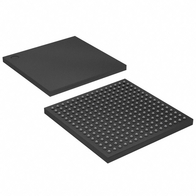
Virtex®-E Field Programmable Gate Array (FPGA) IC 158 65536 1728 240-BFQFP |
|---|---|
| Quantity | 596 Available (as of June 15, 2026) |

| Product Category | Field Programmable Gate Array (FPGA) |
|---|---|
| Manufacturer | AMD |
| Manufacturing Status | Obsolete |
| Manufacturer Standard Lead Time | Contact Us |
| Datasheet |
Specifications & Environmental
| Device Package | 240-PQFP (32x32) | Grade | Commercial | Operating Temperature | 0°C – 85°C | ||
|---|---|---|---|---|---|---|---|
| Package / Case | 240-BFQFP | Number of I/O | 158 | Voltage | 1.71 V - 1.89 V | ||
| Mounting Method | Surface Mount | RoHS Compliance | RoHS non-compliant | REACH Compliance | REACH Unaffected | ||
| Moisture Sensitivity Level | 3 (168 Hours) | Number of LABs/CLBs | 384 | Number of Logic Elements/Cells | 1728 | ||
| Number of Gates | 71693 | ECCN | EAR99 | HTS Code | 8542.39.0001 | ||
| Qualification | N/A | Total RAM Bits | 65536 |
Overview of XCV50E-7PQ240C – Virtex®-E Field Programmable Gate Array (FPGA) IC, 158 I/O, 65,536‑bit RAM, 240‑BFQFP
The XCV50E-7PQ240C is a Virtex®-E 1.8 V FPGA in a 240‑BFQFP surface-mount package targeted for commercial applications. It delivers reprogrammable logic (1,728 logic elements / 71,693 gates) with on-chip RAM and a flexible I/O set for designs that require configurable logic, memory interfacing and high-performance I/O capability.
Built on the Virtex‑E family architecture, this device is suitable for embedded systems, communications and PCI-capable designs that need in-system reconfiguration, deterministic clocking and a compact packaged solution with RoHS compliance.
Key Features
- Core Logic 1,728 logic elements (71,693 gates) providing a reprogrammable logic fabric for custom digital functions.
- On-Chip Memory 65,536 bits of embedded RAM (approximately 0.065 Mbits) for distributed and small block memory requirements.
- I/O Capacity & Differential Support 158 user I/Os. The Virtex‑E family supports high-performance differential standards (LVDS, BLVDS, LVPECL) and high-speed single-ended interfaces, enabling a variety of external interface options.
- Clocking and Timing Architecture-level clock management available in the Virtex‑E family (including multiple DLLs) to support synchronized, high-speed designs.
- Configuration and Re-programmability SRAM-based in-system configuration enables unlimited reprogramming for iterative development and field updates.
- Power and Supply Core voltage supply range: 1.71 V to 1.89 V to match 1.8 V system designs.
- Package & Mounting 240‑BFQFP (surface mount); supplier device package listed as 240‑PQFP (32×32).
- Operating Conditions Commercial temperature grade with an operating range of 0 °C to 85 °C. RoHS compliant.
- Ecosystem Support Virtex‑E family devices are supported by Xilinx development systems and toolchains documented for the series, aiding design integration and verification.
Typical Applications
- Communications Equipment Implements protocol handling, custom interfaces and high-speed data paths using the device’s configurable I/O and logic resources.
- PCI-Based Systems Suitable for designs leveraging the Virtex‑E family’s PCI-compliant interfaces for 3.3 V, 32/64-bit PCI implementations.
- Embedded Processing & Prototyping Reprogrammable logic and in-system configuration make this FPGA useful for iterative embedded designs and hardware/software co-development.
- Memory Interface Prototyping Use the device to prototype high-bandwidth interfaces to external memories and peripherals supported by the Virtex‑E architecture.
Unique Advantages
- Compact, packaged FPGA solution: A 240‑pin BFQFP package delivers a balance of footprint and pin count for space-constrained boards.
- Reprogrammable hardware: SRAM-based configuration enables rapid iteration and field updates without replacing hardware.
- Commercial temperature suitability: Rated for 0 °C to 85 °C operation for mainstream commercial applications.
- Verified family-level feature set: Leverages Virtex‑E series capabilities (advanced memory hierarchy, differential I/O standards, clock-management features) documented for family-level designs.
- Regulatory and manufacturing readiness: RoHS compliance and 100% factory-tested devices simplify environmental and quality compliance considerations.
Why Choose XCV50E-7PQ240C?
The XCV50E-7PQ240C combines the Virtex‑E family’s flexible FPGA architecture with a compact 240‑BFQFP package and a practical set of resources: 1,728 logic elements, approximately 65,536 bits of on-chip RAM, and 158 I/Os. It is positioned for engineers needing a reprogrammable 1.8 V FPGA for commercial designs that demand configurable logic, reliable in-system configuration and a development ecosystem aligned with the Virtex‑E series.
This device fits projects where firmware flexibility, deterministic clocking and a proven family feature set are priorities—offering a scalable approach for prototyping, subsystem integration and mid-density logic implementations.
Request a quote or submit a parts inquiry to check availability and pricing for XCV50E-7PQ240C.


Date Founded: 1969
Headquarters: Santa Clara, California, USA
Employees: 25,000+
Revenue: $22.68 Billion
Certifications and Memberships: ISO9001:2015, RoHS, REACH


