
XCV50E-8CS144C
| Part Description |
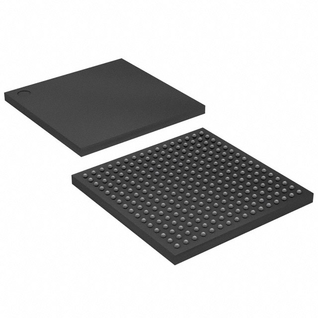
Virtex®-E Field Programmable Gate Array (FPGA) IC 94 65536 1728 144-TFBGA, CSPBGA |
|---|---|
| Quantity | 61 Available (as of June 14, 2026) |

| Product Category | Field Programmable Gate Array (FPGA) |
|---|---|
| Manufacturer | AMD |
| Manufacturing Status | Obsolete |
| Manufacturer Standard Lead Time | Contact Us |
| Datasheet |
Specifications & Environmental
| Device Package | 144-LCSBGA (12x12) | Grade | Commercial | Operating Temperature | 0°C – 85°C | ||
|---|---|---|---|---|---|---|---|
| Package / Case | 144-TFBGA, CSPBGA | Number of I/O | 94 | Voltage | 1.71 V - 1.89 V | ||
| Mounting Method | Surface Mount | RoHS Compliance | RoHS non-compliant | REACH Compliance | REACH Unaffected | ||
| Moisture Sensitivity Level | 3 (168 Hours) | Number of LABs/CLBs | 384 | Number of Logic Elements/Cells | 1728 | ||
| Number of Gates | 71693 | ECCN | EAR99 | HTS Code | 8542.39.0001 | ||
| Qualification | N/A | Total RAM Bits | 65536 |
Overview of XCV50E-8CS144C – Virtex®-E Field Programmable Gate Array (FPGA) IC
The XCV50E-8CS144C is a Virtex®-E family FPGA in a 144-TFBGA/CSPBGA package designed for commercial embedded and system-integration applications. It provides reprogrammable logic resources, on-chip memory, and a broad I/O complement for implementing custom digital functions and protocol interfaces.
Built on the Virtex‑E architecture, the device is suited to designs that require configurable logic capacity, a mix of I/O standards and on-chip RAM. Key electrical and environmental parameters include a VCCINT supply range of 1.71 V to 1.89 V and an operating temperature range of 0 °C to 85 °C.
Key Features
- Logic Capacity — 384 configurable logic blocks (CLBs) providing 1,728 logic elements to implement custom logic, state machines, and glue functions.
- On-chip Memory — 65,536 total RAM bits (approximately 0.06 Mbits) for FIFOs, small buffers, and local data storage.
- I/O Resources — 94 user I/Os to interface with external devices, buses, and signaling standards.
- Gate Count — Approximately 71,693 gates, enabling integration of moderate-complexity digital functions.
- Family-level Capabilities — Built on the Virtex‑E family architecture, which includes high-performance SelectI/O+ technology, differential signaling support, and advanced clock management features described for the Virtex‑E series.
- Package & Mounting — Available in a 144‑TFBGA / CSPBGA form factor with supplier device package listed as 144‑LCSBGA (12×12); surface-mount mounting for compact PCB layouts.
- Power & Temperature — Internal supply voltage specified at 1.71 V–1.89 V and commercial operating temperature range from 0 °C to 85 °C.
- Regulatory — RoHS compliant.
Typical Applications
- Communications & Networking — Implement custom protocol handling, data buffering and interface bridging using the device’s logic elements and on-chip RAM.
- Embedded Systems — Add deterministic custom logic, peripheral glue, and I/O adaptation in compact, board-mounted designs.
- Interface & Bus Conversion — Use the FPGA’s I/O count and family-level SelectI/O features to prototype or deploy signal conversion and timing adaptation between subsystems.
- Prototyping and Development — Reprogrammable logic and moderate memory make the device suitable for iterative design cycles and function emulation in commercial applications.
Unique Advantages
- Balanced Logic and Memory: 1,728 logic elements combined with 65,536 bits of embedded RAM provide a compact platform for mid-range custom logic and buffering tasks.
- Flexible I/O Count: Ninety-four I/Os give designers headroom to connect multiple peripherals, buses, or interfaces without external expander chips.
- Compact BGA Packaging: The 144‑TFBGA/CSPBGA package and surface-mount form factor support dense PCB layouts and small footprint designs.
- Commercial Temperature Rating: Specified 0 °C to 85 °C operation aligns with a wide range of commercial electronics and embedded applications.
- RoHS Compliance: Environmentally compliant manufacturing and materials support current regulatory and assembly practices.
Why Choose XCV50E-8CS144C?
The XCV50E-8CS144C positions itself as a practical, reprogrammable logic device for commercial designs that require a balanced mix of logic elements, on-chip RAM, and a moderate I/O count in a compact BGA package. Its Virtex‑E family heritage provides architecture-level features oriented to flexible I/O and clock management, while the part’s specified electrical and environmental parameters make it straightforward to integrate into commercial embedded systems.
Choose this FPGA when you need a commercially graded, programmable logic element with on-chip memory and a compact package for applications such as interface bridging, custom peripherals, or moderate-complexity digital subsystems.
Request a quote or submit a product inquiry to start the procurement process for XCV50E-8CS144C. Please include required quantities and any packaging or delivery specifications so we can respond promptly.


Date Founded: 1969
Headquarters: Santa Clara, California, USA
Employees: 25,000+
Revenue: $22.68 Billion
Certifications and Memberships: ISO9001:2015, RoHS, REACH


