
XCV600-4BG560I
| Part Description |
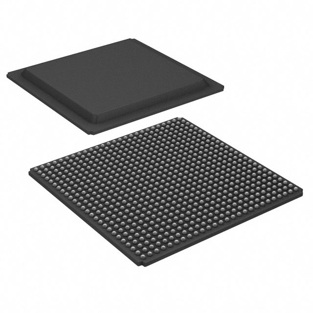
Virtex® Field Programmable Gate Array (FPGA) IC 404 98304 15552 560-LBGA Exposed Pad, Metal |
|---|---|
| Quantity | 92 Available (as of June 18, 2026) |

| Product Category | Field Programmable Gate Array (FPGA) |
|---|---|
| Manufacturer | AMD |
| Manufacturing Status | Obsolete |
| Manufacturer Standard Lead Time | Contact Us |
| Datasheet |
Specifications & Environmental
| Device Package | 560-MBGA (42.5x42.5) | Grade | Industrial | Operating Temperature | -40°C – 100°C | ||
|---|---|---|---|---|---|---|---|
| Package / Case | 560-LBGA Exposed Pad, Metal | Number of I/O | 404 | Voltage | 2.375 V - 2.625 V | ||
| Mounting Method | Surface Mount | RoHS Compliance | RoHS non-compliant | REACH Compliance | REACH Unaffected | ||
| Moisture Sensitivity Level | 3 (168 Hours) | Number of LABs/CLBs | 3456 | Number of Logic Elements/Cells | 15552 | ||
| Number of Gates | 661111 | ECCN | 3A991D | HTS Code | 8542.39.0001 | ||
| Qualification | N/A | Total RAM Bits | 98304 |
Overview of XCV600-4BG560I – Virtex FPGA, Industrial-grade 560-LBGA
The XCV600-4BG560I is an industrial-grade Virtex® Field Programmable Gate Array (FPGA) packaged in a 560-LBGA exposed pad metal case. It delivers a high-density, configurable logic platform suitable for demanding embedded systems and interface-heavy designs. Key strengths include a large logic fabric, on-chip embedded memory, extensive I/O, and integrated clock-management resources to support system-level integration and reprogrammability.
Key Features
- Core Logic 15,552 logic elements (logic cells) and approximately 661,111 system gates provide substantial programmable capacity for complex logic and control functions.
- Embedded Memory Approximately 0.098 Mbits of on-chip RAM (98,304 bits) and hierarchical LUT-based memory options for flexible local storage and buffering.
- I/O and Interface Flexibility 404 user I/O pins and multi-standard SelectIO interfaces supporting 16 high-performance interface standards for diverse external device connectivity.
- Clock Management Built-in clock-management circuitry including four dedicated delay-locked loops (DLLs), four primary low-skew global clock nets, and 24 secondary local clock nets for advanced clock control and low-skew distribution.
- Configuration and Re-programmability SRAM-based in-system configuration with unlimited re-programmability and multiple programming modes for iterative development and field updates.
- Package and Thermal 560-LBGA exposed pad, metal package (supplier device package: 560-MBGA, 42.5 × 42.5 mm) designed for surface-mount assembly and improved thermal conduction.
- Power and Environmental Operating supply range of 2.375 V to 2.625 V, RoHS compliant, and rated for an operating temperature range of −40 °C to 100 °C.
- Fabric and Performance Flexible architecture with dedicated carry logic, multiplier support, abundant registers with clock enable and synchronous/asynchronous controls, and support for fast external RAM interfaces.
Typical Applications
- High-speed interface bridging — Use the multi-standard SelectIO and abundant I/O to implement protocol translation and interface adaptation between disparate system components.
- PCI and legacy bus integration — Supports designs requiring PCI-compliant timing or CompactPCI hot-swap capability as part of system-level I/O handling.
- Embedded system acceleration — Implement custom logic, arithmetic pipelines, and memory controllers using the large logic fabric and embedded RAM.
- Prototyping and in-system reconfiguration — SRAM-based configuration enables iterative development and field updates without hardware replacement.
Unique Advantages
- High-density programmable logic: 15,552 logic elements and ~661k system gates provide substantial capacity for complex designs, reducing the need for multiple discrete ICs.
- Flexible I/O support: 404 I/O pins combined with SelectIO multi-standard capability simplify integration with a wide range of peripherals and memories.
- Deterministic clocking: Four DLLs and dedicated global/local clock nets enable precise clock control and low-skew distribution for high-performance timing domains.
- Field-upgradeable platform: SRAM-based in-system configuration and multiple programming modes allow design updates and feature upgrades in production units.
- Industrial temperature rating: Specified for −40 °C to 100 °C operation, suitable for a range of industrial environments.
- Thermally-aware packaging: 560-LBGA exposed pad metal package with a large 42.5 × 42.5 mm footprint supports effective heat dissipation in surface-mount assemblies.
Why Choose XCV600-4BG560I?
The XCV600-4BG560I combines a large, flexible logic fabric with on-chip memory, robust clock management, and extensive I/O to address complex embedded and interface-centric designs. Its industrial temperature rating, RoHS compliance, and surface-mount 560-LBGA package make it suitable for production systems that require reprogrammability and system-level integration.
This device is well suited for engineering teams needing a configurable platform for protocol bridging, custom acceleration, and in-field updates, offering a balance of capacity, configurability, and thermal considerations in a single FPGA component.
Request a quote or submit a procurement inquiry to check availability and pricing for the XCV600-4BG560I.


Date Founded: 1969
Headquarters: Santa Clara, California, USA
Employees: 25,000+
Revenue: $22.68 Billion
Certifications and Memberships: ISO9001:2015, RoHS, REACH


