
XCV600-4FG676I
| Part Description |
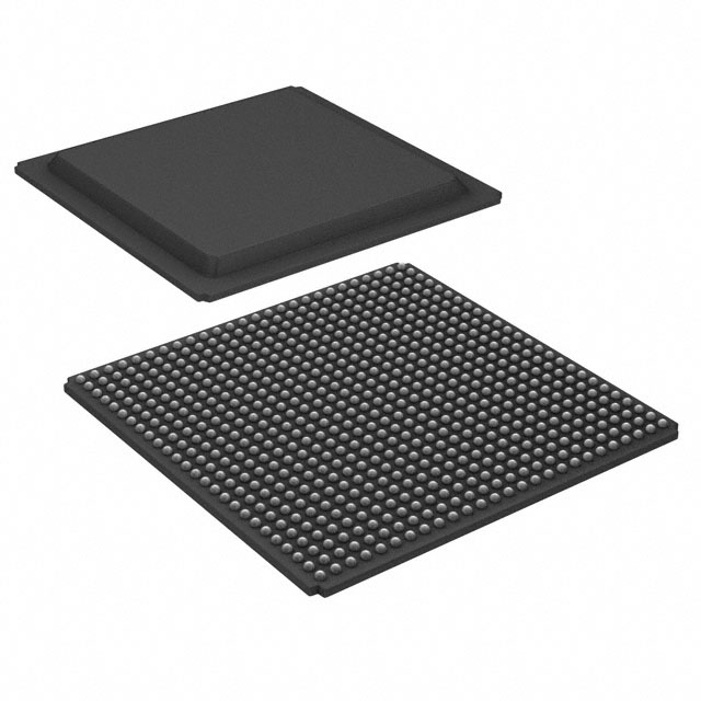
Virtex® Field Programmable Gate Array (FPGA) IC 444 98304 15552 676-BGA |
|---|---|
| Quantity | 192 Available (as of June 10, 2026) |
| Product Category | Field Programmable Gate Array (FPGA) |
|---|---|
| Manufacturer | AMD |
| Manufacturing Status | Obsolete |
| Manufacturer Standard Lead Time | Contact Us |
| Datasheet |
Specifications & Environmental
| Device Package | 676-FBGA (27x27) | Grade | Industrial | Operating Temperature | -40°C – 100°C | ||
|---|---|---|---|---|---|---|---|
| Package / Case | 676-BGA | Number of I/O | 444 | Voltage | 2.375 V - 2.625 V | ||
| Mounting Method | Surface Mount | RoHS Compliance | RoHS non-compliant | REACH Compliance | REACH Unaffected | ||
| Moisture Sensitivity Level | 3 (168 Hours) | Number of LABs/CLBs | 3456 | Number of Logic Elements/Cells | 15552 | ||
| Number of Gates | 661111 | ECCN | 3A991D | HTS Code | 8542.39.0001 | ||
| Qualification | N/A | Total RAM Bits | 98304 |
Overview of XCV600-4FG676I – Virtex® Field Programmable Gate Array (FPGA) IC 444 98304 15552 676-BGA
The XCV600-4FG676I is an industrial-grade, SRAM-based Virtex FPGA designed for high-capacity, in-system programmable logic. It provides a programmable fabric with 15,552 logic cells and on-chip embedded memory suitable for advanced control, data processing, and interface applications.
Built on the Virtex architecture, this device targets designs that require reprogrammability, flexible I/O standards, and clock management for synchronous high-speed systems across industrial temperature ranges.
Key Features
- Logic Capacity — 15,552 logic cells providing a programmable fabric for complex digital designs and system integration.
- Embedded Memory — Approximately 98 kbits of total on-chip RAM bits for LUT-configured RAM and block RAM usage.
- I/O — 444 user I/O pins to support a wide variety of external peripherals and interfaces.
- Clocking and Timing — Built-in clock-management circuitry including four dedicated delay-locked loops (DLLs), four primary low-skew global clock distribution nets and 24 secondary local clock nets for advanced clock control.
- Flexible Logic Architecture — Dedicated carry logic, multiplier support, cascade chains for wide functions, abundant registers with clock enable and set/reset options, and internal 3-state bussing for complex arithmetic and control logic.
- Configurable LUTs and RAM — LUTs configurable as 16-bit/32-bit RAM, dual-ported RAM, or shift registers, plus configurable synchronous dual-ported 4k-bit RAM blocks for hierarchical memory implementations.
- Multi-standard I/O — SelectIO interfaces supporting multiple high-performance interface standards; the family documentation cites direct connectivity options to ZBTRAM-type devices.
- In-System Configuration — SRAM-based architecture enables unlimited re-programmability with multiple programming modes (SelectMAP™, JTAG, master/slave serial modes).
- Package & Mounting — Surface-mount 676-ball BGA (676-FBGA, 27 × 27 mm body) for high-density board integration.
- Electrical & Environmental — Supply range of 2.375 V to 2.625 V and industrial operating temperature from −40°C to 100°C; RoHS compliant.
- Quality & Process — 0.22 μm CMOS process with five-layer metal and 100% factory-tested devices.
- Standards & System Support — Family-level support includes features such as IEEE 1149.1 boundary-scan and design support through Xilinx Foundation/Alliance tool flows; family documentation notes system performance up to 200 MHz and 66-MHz PCI compliance for applicable designs.
Typical Applications
- PCI/Compact PCI Subsystems — Implement custom logic, bridging, or protocol handling for PCI-based cards; family documentation includes PCI compliance and Compact PCI hot-swap support.
- High-speed Data Processing — Use the device’s dedicated carry and multiplier logic plus embedded RAM for packet processing, DSP pre-processing, and mid-stream data tasks.
- Industrial Control & Automation — Industrial-grade temperature range and flexible I/O make the FPGA suitable for control logic, sensor interfacing, and machine I/O aggregation.
- Memory Interface and Buffering — Configurable RAM and fast interfaces support designs that require tight coupling to external high-performance memory devices.
Unique Advantages
- Reprogrammable Flexibility: SRAM-based in-system configuration enables design updates and iterative development without hardware changes.
- Integrated Clock Management: Multiple DLLs and dedicated clock nets simplify timing architecture for multi-clock-domain designs.
- High Logic Density: 15,552 logic cells provide room for complex state machines, datapaths, and custom accelerators in a single device.
- Robust Industrial Operation: Specified −40°C to 100°C operating range supports deployment in temperature-demanding environments.
- Compact, High-density Packaging: 676-ball FBGA package enables dense board-level integration while exposing a large number of user I/Os.
- Proven Silicon and Test Coverage: Fabricated on a 0.22 μm, 5-layer-metal process and 100% factory tested for production reliability.
Why Choose XCV600-4FG676I?
The XCV600-4FG676I combines substantial logic capacity, embedded memory, and flexible I/O in an industrial-grade Virtex FPGA package. Its on-chip clock management, arithmetic acceleration features, and reprogrammable SRAM fabric make it well suited to engineers implementing complex control systems, data-path acceleration, and system interface functions where in-field updates and deterministic timing are required.
Designed for integration into compact, high-density boards, this device offers a balance of performance, programmability, and industrial operating range, backed by the Virtex family’s toolchain and architectural features to support scalable designs and long-term maintainability.
Request a quote or submit a purchase inquiry to obtain pricing, lead time, and availability for XCV600-4FG676I.


Date Founded: 1969
Headquarters: Santa Clara, California, USA
Employees: 25,000+
Revenue: $22.68 Billion
Certifications and Memberships: ISO9001:2015, RoHS, REACH


