
XCV600-5BG432I
| Part Description |
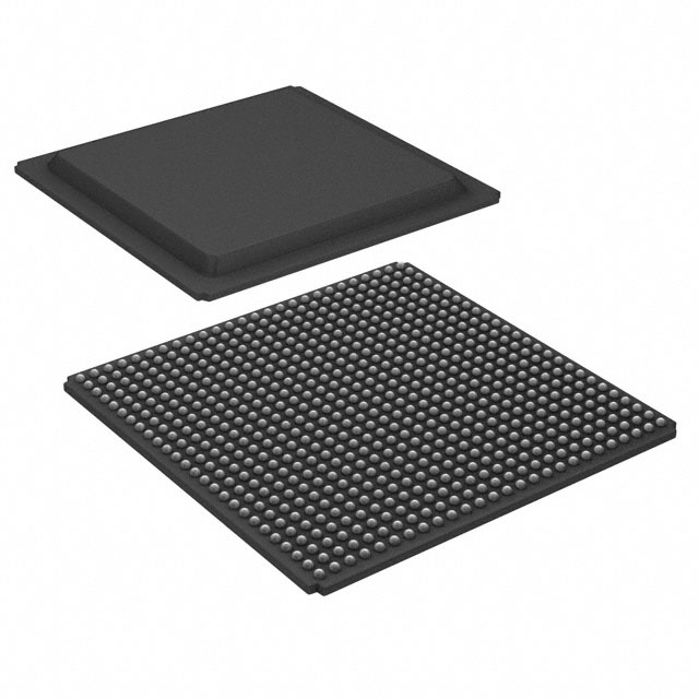
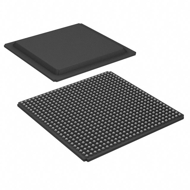
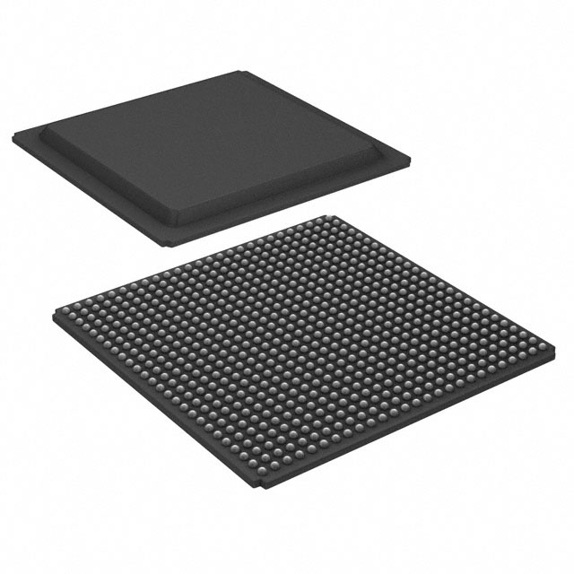
Virtex® Field Programmable Gate Array (FPGA) IC 316 98304 15552 432-LBGA Exposed Pad, Metal |
|---|---|
| Quantity | 30 Available (as of October 7, 2026) |

| Product Category | Field Programmable Gate Array (FPGA) |
|---|---|
| Manufacturer | AMD |
| Manufacturing Status | Obsolete |
| Manufacturer Standard Lead Time | Contact Us |
| Datasheet |
Specifications & Environmental
| Device Package | 432-MBGA (40x40) | Grade | Industrial | Operating Temperature | -40°C – 100°C | ||
|---|---|---|---|---|---|---|---|
| Package / Case | 432-LBGA Exposed Pad, Metal | Number of I/O | 316 | Voltage | 2.375 V - 2.625 V | ||
| Mounting Method | Surface Mount | RoHS Compliance | RoHS non-compliant | REACH Compliance | REACH Unaffected | ||
| Moisture Sensitivity Level | 3 (168 Hours) | Number of LABs/CLBs | 3456 | Number of Logic Elements/Cells | 15552 | ||
| Number of Gates | 661111 | ECCN | 3A991D | HTS Code | 8542.39.0001 | ||
| Qualification | N/A | Total RAM Bits | 98304 |
Overview of XCV600-5BG432I – Virtex® Field Programmable Gate Array (FPGA), 15,552 logic elements, 432‑LBGA
The XCV600-5BG432I is an SRAM-based Virtex FPGA offered in a 432‑LBGA exposed‑pad metal package for surface‑mount assembly. It combines a flexible, regular FPGA architecture with on-chip memory and a broad set of system features to address high‑density programmable logic applications in industrial temperature environments.
Designed for applications that require mid-range logic capacity, abundant I/O and on‑chip RAM, this device supports reprogrammable in‑system configuration and integrates clock management and multi‑standard I/O capabilities for complex digital designs.
Key Features
- Logic Capacity — 15,552 logic elements (CLB‑based architecture) with a reported 661,111 system gates, suitable for medium‑to‑large FPGA designs.
- Embedded Memory — Approximately 0.098 Mbits (98,304 bits) of on‑chip RAM for data buffering, state storage and small memory structures.
- I/O Density — 316 user I/O pins to connect peripherals, buses and external memory interfaces.
- Clock Management — Built‑in clock‑management circuitry including dedicated delay‑locked loops (DLLs) and multiple global/local clock distribution nets as described in the Virtex family specification.
- Flexible Logic and Arithmetic Support — Architecture includes dedicated carry logic, multiplier support and register resources for high‑speed arithmetic and wide‑function implementations (per Virtex family documentation).
- Packaging & Mounting — 432‑LBGA exposed pad, metal package (supplier package: 432‑MBGA, 40×40) for surface‑mount assembly and thermal conduction.
- Power & Supply — Core supply range specified at 2.375 V to 2.625 V.
- Operating Range — Industrial operating temperature range from −40 °C to 100 °C and 100% factory tested per the Virtex family specification.
- Configuration — SRAM‑based in‑system configuration with multiple programming modes and unlimited re‑programmability as described for the Virtex family.
- Process Technology — Implemented on a 0.22 μm, 5‑layer metal CMOS process (Virtex family detail).
- Compliance — RoHS compliant.
Typical Applications
- PCI‑based systems — Suitable for designs that require 66‑MHz PCI compliance and interfacing to system buses and peripherals.
- Compact PCI modules — Supports hot‑swappable Compact PCI applications where reprogrammable logic and in‑system configuration are needed.
- High‑speed arithmetic and DSP logic — Built‑in multiplier and dedicated carry logic make it a fit for compute‑intensive custom processing blocks.
- Memory‑interfacing controllers — Hierarchical memory resources and fast external RAM interfaces enable controllers and buffering logic for memory subsystems.
Unique Advantages
- Reprogrammable in‑system logic: SRAM‑based configuration allows design updates and field reprogramming without hardware changes.
- Balanced capacity and I/O: 15,552 logic elements with 316 I/O pins delivers a compromise of logic density and connectivity for mixed signal/control systems.
- Integrated clocking resources: On‑die DLLs and multiple global/local clock nets simplify clock distribution and timing management within complex designs.
- Industrial temperature rating: Specified operation from −40 °C to 100 °C supports deployment in industrial environments.
- Thermally considerate package: 432‑LBGA exposed pad metal package supports surface‑mount thermal handling for higher‑power designs.
Why Choose XCV600-5BG432I?
The XCV600-5BG432I positions itself as a mid‑to‑high capability Virtex FPGA option that combines substantial logic resources, embedded RAM and plentiful I/O in a robust industrial‑rated package. Its SRAM‑based architecture and onboard clock‑management features enable flexible system design and in‑field updates, while the exposed‑pad LBGA supports thermal considerations of dense implementations.
This device is well suited to engineering teams building PCI/Compact‑PCI modules, custom processing blocks, memory interface controllers and other applications that require reprogrammability, moderate logic capacity and industrial temperature operation backed by the Virtex family feature set.
Request a quote or submit an inquiry to obtain pricing, availability and additional ordering information for the XCV600-5BG432I.




















Date Founded: 1969
Headquarters: Santa Clara, California, USA
Employees: 25,000+
Revenue: $22.68 Billion
Certifications and Memberships: ISO9001:2015, RoHS, REACH











