
XCV600-5FG676C
| Part Description |
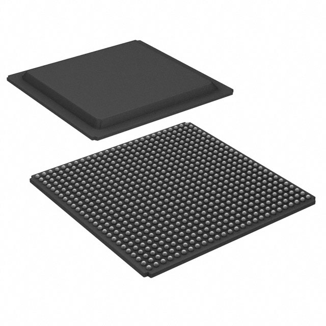
Virtex® Field Programmable Gate Array (FPGA) IC 444 98304 15552 676-BGA |
|---|---|
| Quantity | 1,945 Available (as of June 18, 2026) |

| Product Category | Field Programmable Gate Array (FPGA) |
|---|---|
| Manufacturer | AMD |
| Manufacturing Status | Obsolete |
| Manufacturer Standard Lead Time | Contact Us |
| Datasheet |
Specifications & Environmental
| Device Package | 676-FBGA (27x27) | Grade | Commercial | Operating Temperature | 0°C – 85°C | ||
|---|---|---|---|---|---|---|---|
| Package / Case | 676-BGA | Number of I/O | 444 | Voltage | 2.375 V - 2.625 V | ||
| Mounting Method | Surface Mount | RoHS Compliance | RoHS non-compliant | REACH Compliance | REACH Unaffected | ||
| Moisture Sensitivity Level | 3 (168 Hours) | Number of LABs/CLBs | 3456 | Number of Logic Elements/Cells | 15552 | ||
| Number of Gates | 661111 | ECCN | 3A991D | HTS Code | 8542.39.0001 | ||
| Qualification | N/A | Total RAM Bits | 98304 |
Overview of XCV600-5FG676C – Virtex® 2.5 V FPGA, 676-BGA, 15,552 logic elements
The XCV600-5FG676C is a Virtex® family field-programmable gate array (FPGA) offering 15,552 logic elements and 661,111 system gates in a 676-ball BGA package. This SRAM-based device provides in-system configurability and is targeted at commercial electronic systems requiring mid-to-high logic density, extensive I/O, and flexible clocking and memory resources.
Key hardware characteristics include 444 I/O pins, approximately 0.098 Mbits of embedded memory, a 2.375 V to 2.625 V supply range, and a commercial operating range of 0 °C to 85 °C. The device is RoHS compliant and designed for surface-mount assembly in a 676-FBGA (27×27) footprint.
Key Features
- Core Density & Logic 15,552 logic elements and 661,111 system gates deliver substantial programmable logic capacity for complex custom functions.
- Embedded Memory Approximately 0.098 Mbits of on-chip RAM and configurable LUT-based RAM options support local data buffering and fast on-chip storage.
- I/O & Interface Support 444 general-purpose I/Os and multi-standard SelectIO™ support (family-level feature) enable connectivity to a range of external devices and signaling standards.
- Clock Management Four dedicated delay-locked loops (DLLs) with multiple global and local clock distribution nets provide advanced clock control and low-skew routing.
- Arithmetic & Logic Support Dedicated carry logic, multiplier support, and cascade chains facilitate efficient implementation of high-speed arithmetic and wide-input functions.
- In-System Configuration SRAM-based architecture with unlimited re-programmability and four programming modes allows flexible development and field updates.
- Package & Mounting 676-BGA package (supplier device package: 676-FBGA, 27×27) optimized for surface-mount PCB assembly.
- Power & Operating Range Voltage supply range 2.375 V to 2.625 V and commercial operating temperature of 0 °C to 85 °C.
- Regulatory & Process RoHS compliant; built on a 0.22 µm, 5-layer-metal CMOS process and 100% factory tested (family-level information).
Typical Applications
- PCI and Compact PCI Systems Suitable for FPGA roles in PCI-compliant designs and Compact PCI applications where hot-swap and board-level reconfiguration are required (family-level PCI support noted).
- High-performance Embedded Systems Implement custom control, data parsing, and acceleration logic where significant on-chip logic and local memory are required.
- Networking & Telecom Modules Provide packet processing, protocol bridging, and interface adaptation using abundant I/O and programmable logic resources.
- Prototyping & In-system Upgradable Designs Ideal for development platforms and products that benefit from unlimited re-programmability and multiple configuration modes.
Unique Advantages
- High Logic Capacity: 15,552 logic elements and 661,111 system gates deliver the resources needed for complex, multi-function designs.
- Flexible I/O Integration: 444 pins and family SelectIO capabilities simplify interfacing to diverse peripherals and memory devices.
- Advanced Clocking Topology: Four DLLs and multiple global/local clock nets reduce clock skew and support sophisticated timing architectures.
- Field Re-programmability: SRAM-based configuration with unlimited re-programmability and four programming modes supports iterative development and field updates.
- Commercial Temperature Rating: Specified 0 °C to 85 °C operation for mainstream commercial products.
- RoHS Compliant & Factory Tested: Meets RoHS requirements and is 100% factory tested at the family level.
Why Choose XCV600-5FG676C?
The XCV600-5FG676C positions itself as a robust, mid-to-high density Virtex FPGA option for commercial electronic designs that require significant programmable logic, rich I/O, and flexible clock and memory resources. Its SRAM-based re-programmability and family-level design features provide designers with a versatile platform for prototyping, system integration, and field-updatable products.
Supported by the Virtex design ecosystem and development tools (family-level support), this device offers a balance of integration, configurability, and tested manufacturing that helps reduce development time while enabling scalable design growth.
If you would like pricing information or to request a formal quote for the XCV600-5FG676C, submit a request and our team will respond with availability and ordering details.


Date Founded: 1969
Headquarters: Santa Clara, California, USA
Employees: 25,000+
Revenue: $22.68 Billion
Certifications and Memberships: ISO9001:2015, RoHS, REACH


