
XCV600-5FG680C
| Part Description |
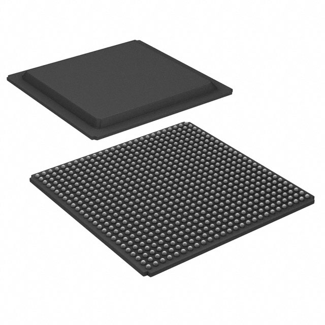
Virtex® Field Programmable Gate Array (FPGA) IC 512 98304 15552 680-LBGA Exposed Pad |
|---|---|
| Quantity | 421 Available (as of June 15, 2026) |

| Product Category | Field Programmable Gate Array (FPGA) |
|---|---|
| Manufacturer | AMD |
| Manufacturing Status | Obsolete |
| Manufacturer Standard Lead Time | Contact Us |
| Datasheet |
Specifications & Environmental
| Device Package | 680-FTEBGA (40x40) | Grade | Commercial | Operating Temperature | 0°C – 85°C | ||
|---|---|---|---|---|---|---|---|
| Package / Case | 680-LBGA Exposed Pad | Number of I/O | 512 | Voltage | 2.375 V - 2.625 V | ||
| Mounting Method | Surface Mount | RoHS Compliance | RoHS non-compliant | REACH Compliance | REACH Unaffected | ||
| Moisture Sensitivity Level | 3 (168 Hours) | Number of LABs/CLBs | 3456 | Number of Logic Elements/Cells | 15552 | ||
| Number of Gates | 661111 | ECCN | 3A001A7A | HTS Code | 8542.39.0001 | ||
| Qualification | N/A | Total RAM Bits | 98304 |
Overview of XCV600-5FG680C – Virtex® FPGA, 15,552 logic elements, 680-LBGA
The XCV600-5FG680C is a high-density, SRAM-based Field Programmable Gate Array (FPGA) offered in a 680-LBGA exposed pad package. It delivers 15,552 logic elements, 512 user I/O pins, and approximately 0.098 Mbits of embedded RAM, making it suitable for complex digital systems that require reprogrammable logic and flexible I/O connectivity.
Designed for commercial-grade applications, this device targets high-performance interfaces, in-system reconfiguration, and designs that benefit from abundant on-chip logic and memory resources while operating within a 2.375 V to 2.625 V supply range and 0 °C to 85 °C ambient.
Key Features
- High-density programmable logic — 15,552 logic elements and 661,111 system gates provide significant capacity for complex logic and compute functions.
- Generous I/O count — 512 user I/O pins support wide external interfacing and multiple concurrent peripheral connections.
- Embedded memory — 98,304 total RAM bits (approximately 0.098 Mbits) and a hierarchical memory architecture with LUTs configurable as various RAM types and 4k-bit dual-ported RAM blocks.
- Clock management — Dedicated clock resources including four delay-locked loops (DLLs), four primary low-skew global clock nets, and 24 secondary local clock nets for advanced timing control.
- Multi-standard I/O — SelectIO™ interfaces supporting multiple high-performance standards for direct connection to a variety of external devices and memories.
- Configuration flexibility — SRAM-based in-system configuration with unlimited re-programmability and multiple programming modes.
- Package and mounting — 680-LBGA exposed pad (supplier package: 680-FTEBGA, 40×40) for surface-mount PCB assembly and thermal conduction.
- Supply and temperature — Operates from 2.375 V to 2.625 V and rated for commercial temperature range (0 °C to 85 °C).
- Manufacturing process — Built on a 0.22 µm, 5-layer metal CMOS process and fully factory tested to ensure device consistency.
- Standards and interoperability — Supports system performance up to the Virtex family guidance and includes features such as 66-MHz PCI compliance and hot-swap support for Compact PCI as indicated in the Virtex product family specification.
- Environmental compliance — RoHS compliant.
Typical Applications
- High-performance interfaces — Use the device’s SelectIO capabilities and high I/O count to implement multi-standard communication front ends and protocol bridges.
- System prototyping and FPGA-based emulation — Reconfigurable logic and in-system programming modes enable iterative hardware development and rapid design validation.
- Embedded memory-centric designs — The hierarchical memory resources and configurable LUT RAM support on-chip buffering, small FIFOs, and local data storage for DSP or control tasks.
- PCI and Compact PCI systems — Built-in compatibility with 66-MHz PCI and hot-swap support aligns the device for use in Compact PCI and related backplane applications.
Unique Advantages
- Significant logic capacity: 15,552 logic elements and 661,111 gates give designers room to implement complex custom logic without immediate part upgrades.
- Flexible memory topology: Approximately 0.098 Mbits of on-chip RAM and configurable LUT-based RAM allow designers to tailor memory use to application needs.
- Robust clocking resources: Multiple DLLs and dedicated clock nets simplify timing architectures for high-speed designs.
- Wide I/O capability: 512 user I/Os enable broad external interfacing options, reducing the need for external buffering or GPIO expanders.
- Commercial-grade readiness: Surface-mount 680-LBGA package with exposed pad and RoHS compliance facilitates standard PCB assembly and regulatory alignment.
- In-system reprogrammability: SRAM-based configuration and multiple programming modes streamline firmware updates and field revisions.
Why Choose XCV600-5FG680C?
The XCV600-5FG680C offers a balanced combination of logic density, memory resources, and extensive I/O in a commercial-grade FPGA package. Its dedicated clock management, configurable on-chip RAM, and multi-standard SelectIO support make it well suited for engineers implementing complex interface logic, prototyping advanced systems, or deploying reprogrammable functions on existing PCBs.
Backed by factory testing and a mature Virtex family architecture, the device provides predictable behavior for long-term designs where reprogrammability, integration, and a high I/O count are priorities. Its voltage and temperature specifications align with standard commercial system environments, delivering a dependable platform for a wide range of embedded and communication applications.
Request a quote or submit an inquiry to receive pricing and availability information for the XCV600-5FG680C and to discuss how it can fit into your next design.


Date Founded: 1969
Headquarters: Santa Clara, California, USA
Employees: 25,000+
Revenue: $22.68 Billion
Certifications and Memberships: ISO9001:2015, RoHS, REACH


