
XCV600-5FG680I
| Part Description |
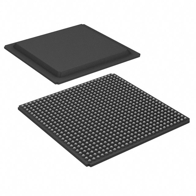
Virtex® Field Programmable Gate Array (FPGA) IC 512 98304 15552 680-LBGA Exposed Pad |
|---|---|
| Quantity | 1,183 Available (as of June 18, 2026) |

| Product Category | Field Programmable Gate Array (FPGA) |
|---|---|
| Manufacturer | AMD |
| Manufacturing Status | Obsolete |
| Manufacturer Standard Lead Time | Contact Us |
| Datasheet |
Specifications & Environmental
| Device Package | 680-FTEBGA (40x40) | Grade | Industrial | Operating Temperature | -40°C – 100°C | ||
|---|---|---|---|---|---|---|---|
| Package / Case | 680-LBGA Exposed Pad | Number of I/O | 512 | Voltage | 2.375 V - 2.625 V | ||
| Mounting Method | Surface Mount | RoHS Compliance | RoHS non-compliant | REACH Compliance | REACH Unaffected | ||
| Moisture Sensitivity Level | 3 (168 Hours) | Number of LABs/CLBs | 3456 | Number of Logic Elements/Cells | 15552 | ||
| Number of Gates | 661111 | ECCN | 3A001A7A | HTS Code | 8542.39.0001 | ||
| Qualification | N/A | Total RAM Bits | 98304 |
Overview of XCV600-5FG680I – Virtex® Field Programmable Gate Array (FPGA) IC 512 98304 15552 680-LBGA Exposed Pad
The XCV600-5FG680I is an SRAM-based Virtex® FPGA offering a high-capacity, high-performance programmable-logic fabric optimized for system-level designs. Its architecture combines abundant logic resources, a hierarchical memory system, and multi-standard I/O to address applications that require reprogrammable, high-density logic.
Designed for industrial environments, this device delivers a balance of integration and configurability through features such as on-chip embedded memory, dedicated clock-management circuitry, and flexible I/O support.
Key Features
- Logic Capacity — 15,552 logic elements, enabling implementation of substantial custom logic and complex functions.
- On-chip Memory — Approximately 0.098 Mbits of embedded memory (98,304 bits) for block RAM and SelectRAM+ usage to support data buffering and local storage.
- I/O Density — 512 user I/O pins suitable for wide parallel interfaces and system-level connectivity.
- System Gates — Approximately 661,111 system gates for estimating overall design scale and integration.
- Clock Management — Four dedicated delay-locked loops (DLLs) with four primary low-skew global clock nets plus 24 secondary local clock nets for advanced clock distribution and timing control.
- Multi-standard SelectIO — Support for multiple high-performance interface standards and direct connection options to external ZBTRAM devices.
- Flexible Memory Architecture — LUTs configurable as 16-bit/32-bit RAM, dual-ported RAM, or shift registers, and configurable synchronous dual-ported 4k-bit RAMs for varied memory-use cases.
- Process and Testing — Built on a 0.22 μm, 5-layer-metal CMOS process and 100% factory tested.
- Package and Mounting — 680-LBGA exposed pad package (supplier device package: 680-FTEBGA, 40×40); surface-mount mounting type.
- Power and Temperature — Supported supply range 2.375 V to 2.625 V; operating temperature −40 °C to 100 °C (industrial grade).
- Configuration — SRAM-based in-system configuration with unlimited re-programmability and multiple programming modes.
- Additional System Features — Dedicated carry logic, multiplier support, cascade chains for wide functions, internal 3-state bussing, IEEE 1149.1 boundary-scan logic, and a die-temperature sensor diode.
- Performance — System performance figures referenced in product documentation (for example, up to 200 MHz system performance and 66-MHz PCI compliance where applicable).
Typical Applications
- PCI and CompactPCI Systems — Implementation of PCI-compliant logic and hot-swappable CompactPCI interfaces, leveraging the device’s interface standards and timing resources.
- High-density Custom Logic — Replacement of mask-programmed gate arrays in designs that benefit from reprogrammability and high gate count.
- Memory-Intensive Control and Buffering — Local data storage and buffering using the hierarchical on-chip memory and SelectRAM+ capabilities.
- Clock-critical Systems — Designs requiring advanced clock control and low-skew distribution using the device’s DLLs and global/local clock nets.
Unique Advantages
- Highly Reconfigurable: SRAM-based architecture with unlimited re-programmability enables iterative development and in-field updates without hardware changes.
- Balanced Speed and Density: High logic element count and dedicated arithmetic resources support complex, high-performance functions while managing silicon area.
- Robust Clocking: Four DLLs and multiple global/local clock nets simplify timing closure and deliver controlled clock distribution for synchronized systems.
- Comprehensive I/O Support: 512 I/O pins and multi-standard SelectIO interfaces streamline integration with external memory and peripheral devices.
- Industrial Temperature Range: Specified operation from −40 °C to 100 °C supports deployment in industrial environments requiring extended temperature capability.
- Proven Manufacturing and Test: 0.22 μm, 5-layer-metal process and 100% factory testing help ensure consistent device quality.
Why Choose XCV600-5FG680I?
The XCV600-5FG680I provides a large, flexible FPGA fabric with a combination of logic density, embedded memory, and advanced clock and I/O resources suited to demanding, reprogrammable system designs. Its industrial temperature rating, surface-mount 680-LBGA package, and validated process/testing pedigree make it appropriate for designs where robustness and configurability are required.
This device is well matched to teams and projects that need to migrate or replace mask-programmed logic, implement complex interface logic, or iterate hardware functionality in-field—while maintaining a clear path for scaling within the Virtex family architecture documented in product literature.
Request a quote or submit your requirements to receive pricing and availability for the XCV600-5FG680I. Include your desired quantity and target lead time for the fastest response.


Date Founded: 1969
Headquarters: Santa Clara, California, USA
Employees: 25,000+
Revenue: $22.68 Billion
Certifications and Memberships: ISO9001:2015, RoHS, REACH


