
XCV600-5HQ240I
| Part Description |
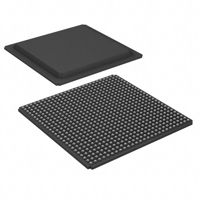
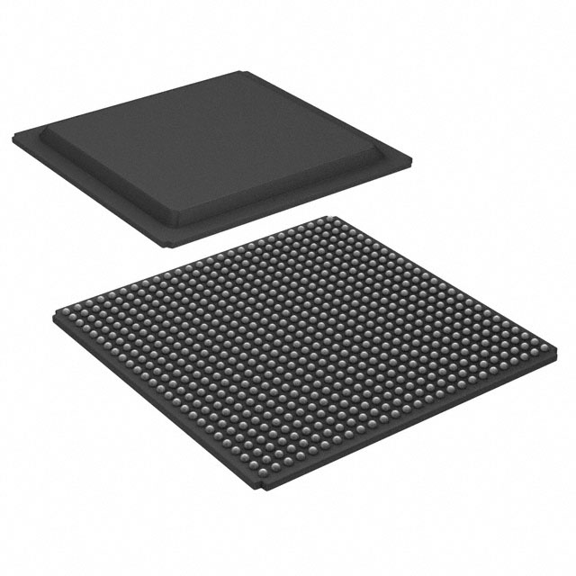
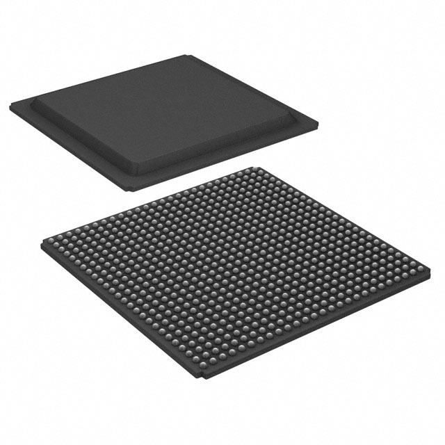
Virtex® Field Programmable Gate Array (FPGA) IC 166 98304 15552 240-BFQFP Exposed Pad |
|---|---|
| Quantity | 1,139 Available (as of October 8, 2026) |

| Product Category | Field Programmable Gate Array (FPGA) |
|---|---|
| Manufacturer | AMD |
| Manufacturing Status | Obsolete |
| Manufacturer Standard Lead Time | Contact Us |
| Datasheet |
Specifications & Environmental
| Device Package | 240-PQFP (32x32) | Grade | Industrial | Operating Temperature | -40°C – 100°C | ||
|---|---|---|---|---|---|---|---|
| Package / Case | 240-BFQFP Exposed Pad | Number of I/O | 166 | Voltage | 2.375 V - 2.625 V | ||
| Mounting Method | Surface Mount | RoHS Compliance | RoHS non-compliant | REACH Compliance | REACH Unaffected | ||
| Moisture Sensitivity Level | 3 (168 Hours) | Number of LABs/CLBs | 3456 | Number of Logic Elements/Cells | 15552 | ||
| Number of Gates | 661111 | ECCN | 3A001A7B | HTS Code | 8542.39.0001 | ||
| Qualification | N/A | Total RAM Bits | 98304 |
Overview of XCV600-5HQ240I – Virtex® Field Programmable Gate Array (FPGA) IC 166 98304 15552 240-BFQFP Exposed Pad
The XCV600-5HQ240I is a Virtex® family SRAM-based Field Programmable Gate Array (FPGA) offered by AMD, optimized for high-capacity, reconfigurable digital logic. It delivers 15,552 logic elements, approximately 98,304 bits of embedded memory, and 166 user I/O pins in a 240-BFQFP exposed pad package, serving applications that require dense logic, flexible on-chip memory and robust I/O in an industrial-grade device.
Designed with integrated clock management and advanced routing resources, this device targets high-performance prototyping, embedded logic acceleration, and interface-centric applications that benefit from in-system programmability and a mature FPGA development ecosystem.
Key Features
- Logic Capacity — 15,552 logic elements and 661,111 system gates provide significant on-chip logic resources for complex designs.
- On-chip Memory — Approximately 98,304 bits of embedded RAM, plus flexible LUT-based memory configurations for data buffering and state storage.
- I/O and Interfaces — 166 user I/O pins available in a 240-BFQFP exposed pad package, supporting a broad range of external device connections.
- Clock Management — Built-in clock-management circuitry including four dedicated delay-locked loops (DLLs) and multiple global/secondary clock distribution nets for advanced clock control.
- SRAM-based In-System Configuration — Re-programmable architecture with four programming modes and support for loading configuration from external PROM or via configuration interfaces.
- Process and Test — Implemented in a 0.22 μm, 5-layer-metal CMOS process and 100% factory tested for production reliability.
- Electrical and Thermal — Supply voltage range of 2.375 V to 2.625 V and operating temperature from −40 °C to 100 °C for industrial environments.
- Package & Mounting — Surface-mount 240-BFQFP exposed pad (240-PQFP, 32×32) for high-pin-count designs and thermal dissipation via exposed pad.
- Compliance — RoHS compliant, supporting environmental requirements in modern electronics manufacturing.
Typical Applications
- High-performance prototyping — Rapid hardware development and iteration using a re-programmable SRAM-based FPGA with substantial logic and on-chip memory.
- Interface bridging and protocol implementation — Implement custom I/O protocols or translate between high-density interfaces using abundant I/O and flexible routing.
- Embedded system acceleration — Offload compute-intensive or timing-critical functions to the FPGA fabric leveraging dedicated arithmetic and memory resources.
- PCI and Compact PCI systems — Suitable for designs that require 66-MHz PCI compatibility and support for hot-swappable Compact PCI modules as indicated in the device family specification.
Unique Advantages
- High logic density: 15,552 logic elements and 661,111 system gates enable consolidation of complex functions onto a single device, reducing BOM and board area.
- Flexible on-chip memory: Approximately 98,304 bits of embedded RAM and configurable LUT-based memory modes support varied buffering and state-storage needs without external RAM.
- Advanced clock control: Four dedicated DLLs and multiple clock distribution nets provide robust options for managing multi-domain timing and low-skew clocking.
- Industrial temperature range: Rated for −40 °C to 100 °C to meet reliable operation across a broad set of deployed environments.
- Proven process and test: 0.22 μm, 5-layer-metal manufacturing and 100% factory testing for predictable production quality.
- Development ecosystem support: Backed by the Virtex family’s development tools and design flows referenced in the product documentation to accelerate time-to-market.
Why Choose XCV600-5HQ240I?
The XCV600-5HQ240I combines sizable logic capacity, flexible embedded memory, and comprehensive clock and I/O resources in a single industrial-grade, surface-mount package. It is well suited for engineers who need a re-programmable platform that balances performance and integration while supporting in-system configuration and multiple programming modes.
This device is appropriate for complex prototyping, interface-intensive designs, and embedded acceleration where predictable supply voltage ranges, extended temperature operation, and RoHS compliance are required. Its inclusion in the Virtex family ensures compatibility with established design tools and methodologies for scalable project development.
Request a quote or submit a procurement inquiry to get pricing, availability, and integration support for the XCV600-5HQ240I.




















Date Founded: 1969
Headquarters: Santa Clara, California, USA
Employees: 25,000+
Revenue: $22.68 Billion
Certifications and Memberships: ISO9001:2015, RoHS, REACH











