
XCV600-5BG432C
| Part Description |
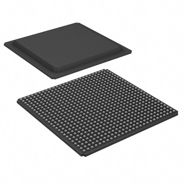
Virtex® Field Programmable Gate Array (FPGA) IC 316 98304 15552 432-LBGA Exposed Pad, Metal |
|---|---|
| Quantity | 1,117 Available (as of June 15, 2026) |

| Product Category | Field Programmable Gate Array (FPGA) |
|---|---|
| Manufacturer | AMD |
| Manufacturing Status | Obsolete |
| Manufacturer Standard Lead Time | Contact Us |
| Datasheet |
Specifications & Environmental
| Device Package | 432-MBGA (40x40) | Grade | Commercial | Operating Temperature | 0°C – 85°C | ||
|---|---|---|---|---|---|---|---|
| Package / Case | 432-LBGA Exposed Pad, Metal | Number of I/O | 316 | Voltage | 2.375 V - 2.625 V | ||
| Mounting Method | Surface Mount | RoHS Compliance | RoHS non-compliant | REACH Compliance | REACH Unaffected | ||
| Moisture Sensitivity Level | 3 (168 Hours) | Number of LABs/CLBs | 3456 | Number of Logic Elements/Cells | 15552 | ||
| Number of Gates | 661111 | ECCN | 3A991D | HTS Code | 8542.39.0001 | ||
| Qualification | N/A | Total RAM Bits | 98304 |
Overview of XCV600-5BG432C – Virtex® 2.5 V Field Programmable Gate Array, 432‑LBGA
The XCV600-5BG432C is a Virtex® FPGA offering high-capacity, high-performance programmable logic in a 432‑ball LBGA package with exposed metal pad. Built on the Virtex architecture, this SRAM-based device delivers reprogrammable system logic with on-chip memory and extensive I/O for complex digital designs in commercial applications.
With 15,552 logic cells, approximately 98,304 bits of embedded RAM, and 316 I/O, the device targets system-level integration tasks such as high-performance interfaces, memory bridging, and reconfigurable logic implementation while operating from a 2.375 V to 2.625 V supply and a 0 °C to 85 °C ambient range.
Key Features
- Logic Capacity: 15,552 logic cells across a 48×72 CLB array (3,456 CLBs) to implement complex combinational and sequential logic.
- Embedded Memory: Approximately 98,304 bits of block RAM and configurable LUT-based RAM options for on-chip data storage and buffering.
- I/O Resources: 316 user I/O pins to support wide external connectivity and high-pin-count interfaces.
- Clock Management: Four dedicated delay-locked loops (DLLs) plus multiple global and local clock distribution nets for flexible, low-skew clocking architectures.
- High-Speed Interfaces: Multi-standard SelectIO™ support and direct connections to ZBT RAM devices; supports PCI-compliant operation at 66 MHz and CompactPCI hot-swap scenarios as documented in the product series.
- Configurable Arithmetic and Logic: Dedicated carry logic, multiplier support and cascade chains for efficient implementation of wide arithmetic and aggregation functions.
- SRAM-Based In-System Configuration: Unlimited re-programmability with multiple programming modes (SelectMAP™, serial, JTAG) for in-system updates and development flexibility.
- Package & Mounting: 432‑LBGA exposed pad, metal package (432‑MBGA footprint 40×40) designed for surface-mount assembly.
- Electrical & Environmental: Core supply range 2.375 V to 2.625 V; commercial grade operation from 0 °C to 85 °C. RoHS compliant.
Typical Applications
- High-performance system logic: Implement custom datapaths, protocol controllers, and glue logic where reconfigurability and dense logic resources are required.
- Memory interfaces and bridging: Use the large I/O count and SelectIO capability for ZBT/external RAM interfacing and memory-controller implementations.
- PCI and CompactPCI subsystems: Leverage documented 66‑MHz PCI compliance and CompactPCI hot-swap support for ruggedized expansion and I/O cards.
- Prototyping and in-system reconfiguration: SRAM-based architecture and multiple configuration modes enable iterative development and field updates without hardware changes.
Unique Advantages
- Reprogrammable Flexibility: SRAM-based in-system configuration enables unlimited re-programmability to iterate designs or deploy updates in the field.
- Balanced Performance and Density: 15,552 logic cells and dedicated arithmetic resources support complex logic while keeping routing and placement efficient.
- Robust Clocking: Four DLLs and hierarchical clock nets provide precise timing control for multi-clock-domain designs.
- Broad I/O Connectivity: 316 I/O pins and multi-standard SelectIO support accommodate a wide range of external devices and interface standards.
- Compact, Assembly-Ready Package: 432-LBGA with exposed pad and surface-mount mounting simplifies thermal management and PCB integration for commercial products.
Why Choose XCV600-5BG432C?
The XCV600-5BG432C provides a capable balance of logic density, embedded memory, and I/O resources in a commercially graded, RoHS-compliant Virtex FPGA. Its SRAM-based architecture and flexible clocking make it suitable for designers who need in-system reconfigurability, dense combinational resources, and reliable clock management for multi-domain systems.
This device is ideal for commercial electronic designs requiring substantial programmable logic capacity, substantial I/O, and on-chip RAM—all packaged for surface-mount assembly. The Virtex family support and documented configuration modes provide a straightforward path for development and deployment.
Request a quote to check current availability and pricing for the XCV600-5BG432C and initiate your design evaluation or procurement process today.


Date Founded: 1969
Headquarters: Santa Clara, California, USA
Employees: 25,000+
Revenue: $22.68 Billion
Certifications and Memberships: ISO9001:2015, RoHS, REACH


