
XCV600-4HQ240C
| Part Description |
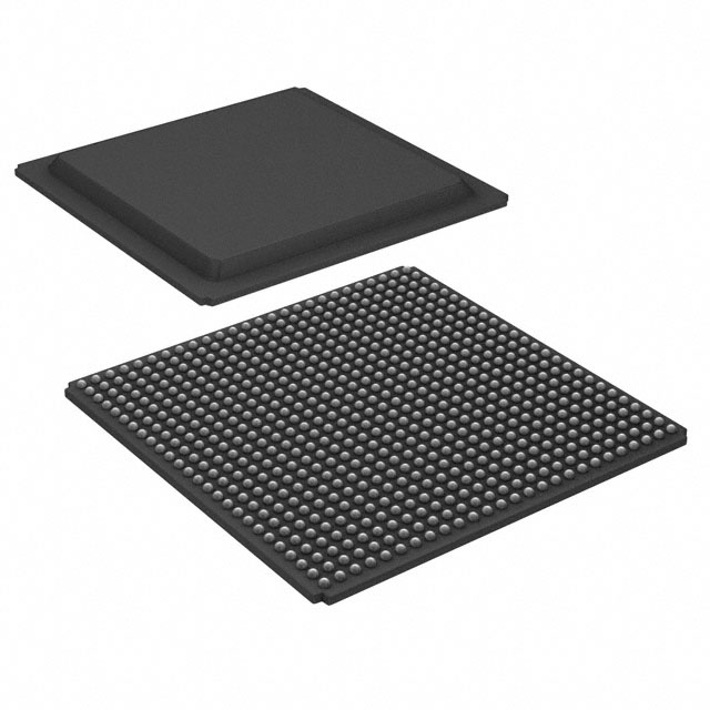
Virtex® Field Programmable Gate Array (FPGA) IC 166 98304 15552 240-BFQFP Exposed Pad |
|---|---|
| Quantity | 113 Available (as of June 14, 2026) |

| Product Category | Field Programmable Gate Array (FPGA) |
|---|---|
| Manufacturer | AMD |
| Manufacturing Status | Obsolete |
| Manufacturer Standard Lead Time | Contact Us |
| Datasheet |
Specifications & Environmental
| Device Package | 240-PQFP (32x32) | Grade | Commercial | Operating Temperature | 0°C – 85°C | ||
|---|---|---|---|---|---|---|---|
| Package / Case | 240-BFQFP Exposed Pad | Number of I/O | 166 | Voltage | 2.375 V - 2.625 V | ||
| Mounting Method | Surface Mount | RoHS Compliance | RoHS non-compliant | REACH Compliance | REACH Unaffected | ||
| Moisture Sensitivity Level | 3 (168 Hours) | Number of LABs/CLBs | 3456 | Number of Logic Elements/Cells | 15552 | ||
| Number of Gates | 661111 | ECCN | 3A001A7B | HTS Code | 8542.39.0001 | ||
| Qualification | N/A | Total RAM Bits | 98304 |
Overview of XCV600-4HQ240C – Virtex® Field Programmable Gate Array (FPGA), 15,552 logic elements, ~0.098 Mbits RAM, 166 I/O, 240-BFQFP
The XCV600-4HQ240C is an AMD Virtex® SRAM-based Field Programmable Gate Array optimized for high-capacity, high-performance programmable logic designs. It provides a flexible, regularly structured architecture suited to complex digital systems that require in-system reprogrammability and advanced clocking control.
With 15,552 logic elements, approximately 0.098 Mbits of embedded memory and 166 I/O pins in a 240-BFQFP exposed pad package, this commercial-grade FPGA targets applications that demand substantial logic capacity, configurable memory resources and robust I/O connectivity within a compact surface-mount footprint.
Key Features
- Logic Capacity Provides 15,552 logic elements and approximately 661,111 system gates for implementing large combinational and sequential logic functions.
- Embedded Memory Includes approximately 98,304 bits of on-chip RAM, enabling local data storage and high-speed buffering inside the FPGA fabric.
- I/O and Connectivity 166 general-purpose I/O pins support diverse interfacing requirements from control signals to parallel/serial links.
- Clock Management Built-in clock-management circuitry at the family level includes dedicated delay-locked loops (DLLs) and hierarchical global/local clock distribution for low-skew clocking and advanced timing control.
- Configurable Logic Fabric Flexible logic blocks support LUT-based RAM and shift-register configurations, cascade chains for wide-input functions, dedicated carry logic and multiplier support for arithmetic-intensive designs.
- Packaging and Mounting 240-BFQFP exposed pad (supplier package: 240-PQFP 32×32) in a surface-mount form factor for compact board integration and thermal conduction through the exposed pad.
- Power and Electrical Device operates from a supply range of 2.375 V to 2.625 V, suitable for compatible system power rails.
- Commercial Grade and Temperature Rated for commercial operation with an operating temperature range of 0 °C to 85 °C.
- Reprogrammability and Configuration SRAM-based architecture enables unlimited re-programmability and multiple programming modes for in-system updates (feature described at the family level).
- Environmental Compliance RoHS compliant for environmental and regulatory alignment.
Typical Applications
- PCI and CompactPCI Systems Suitable for programmable logic functions in PCI-compliant systems and CompactPCI environments that benefit from hot-swappable or reconfigurable logic at the board level.
- High-speed Digital Processing Useful for custom data-paths, signal processing and control logic where substantial on-chip logic and embedded RAM reduce external memory traffic and latency.
- Interface Bridging and Custom I/O With 166 I/O pins, the device is effective for protocol bridging, custom interface implementation and board-level glue logic between disparate subsystems.
- Prototyping and Iterative Design SRAM reprogrammability supports rapid design iteration and prototyping of complex digital systems without mask-programmed ASIC costs.
Unique Advantages
- High Logic Density: 15,552 logic elements and ~661,111 gates provide headroom for complex logic integration, reducing the need for multiple discrete devices.
- Integrated Embedded Memory: Approximately 0.098 Mbits of on-chip RAM enables local buffering and table storage that speed data-paths and reduce external memory dependence.
- Advanced Clocking Support: Family-level clock-management features including dedicated DLLs and hierarchical clock nets help manage timing across large designs.
- Compact Surface-Mount Package: 240-BFQFP exposed pad with a 32×32 supplier package footprint balances I/O count and thermal performance for board-level integration.
- Flexible Configuration: SRAM-based in-system configuration allows multiple programming modes and unlimited re-programmability for design updates and field changes.
- Regulatory Compliance: RoHS compliance supports environmental and manufacturing requirements for commercial products.
Why Choose XCV600-4HQ240C?
The XCV600-4HQ240C positions itself as a robust, reprogrammable logic element for commercial systems that require significant logic capacity, embedded memory and flexible I/O in a compact package. Its combination of substantial logic resources, configurable memory primitives and advanced clocking features addresses designs that need on-board customization, rapid iteration and reliable timing control.
Backed by the Virtex family development ecosystem and built around an SRAM-based architecture, this FPGA is suited for engineering teams developing complex digital subsystems, prototype platforms and reconfigurable interface solutions where long-term flexibility and in-system updates are important.
Request a quote or submit a parts inquiry to receive pricing and availability details for XCV600-4HQ240C and to discuss how this FPGA can fit your next design.


Date Founded: 1969
Headquarters: Santa Clara, California, USA
Employees: 25,000+
Revenue: $22.68 Billion
Certifications and Memberships: ISO9001:2015, RoHS, REACH


