
XCV800-6BG560C
| Part Description |
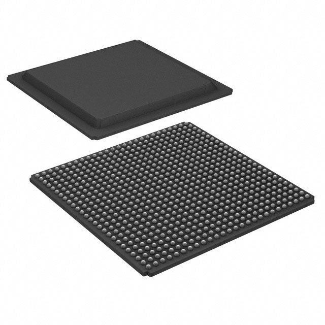
Virtex® Field Programmable Gate Array (FPGA) IC 404 114688 21168 560-LBGA Exposed Pad, Metal |
|---|---|
| Quantity | 1,141 Available (as of June 18, 2026) |

| Product Category | Field Programmable Gate Array (FPGA) |
|---|---|
| Manufacturer | AMD |
| Manufacturing Status | Obsolete |
| Manufacturer Standard Lead Time | Contact Us |
| Datasheet |
Specifications & Environmental
| Device Package | 560-MBGA (42.5x42.5) | Grade | Commercial | Operating Temperature | 0°C – 85°C | ||
|---|---|---|---|---|---|---|---|
| Package / Case | 560-LBGA Exposed Pad, Metal | Number of I/O | 404 | Voltage | 2.375 V - 2.625 V | ||
| Mounting Method | Surface Mount | RoHS Compliance | RoHS non-compliant | REACH Compliance | REACH Unaffected | ||
| Moisture Sensitivity Level | 3 (168 Hours) | Number of LABs/CLBs | 4704 | Number of Logic Elements/Cells | 21168 | ||
| Number of Gates | 888439 | ECCN | 3A991D | HTS Code | 8542.39.0001 | ||
| Qualification | N/A | Total RAM Bits | 114688 |
Overview of XCV800-6BG560C – Virtex® Field Programmable Gate Array, 21,168 logic elements, 114,688 bits RAM, 560-LBGA
The XCV800-6BG560C is an SRAM-based Virtex® FPGA optimized for high-density, reprogrammable logic. It provides 21,168 logic elements, approximately 0.115 Mbits of embedded memory, and 404 user I/O in a 560-ball L-BGA exposed-pad package for surface-mount assembly.
Designed for commercial-temperature applications, this device targets designs that require high logic capacity, flexible I/O, on-chip memory and integrated clock management while operating from a 2.375 V to 2.625 V core supply.
Key Features
- Logic Capacity — 21,168 logic elements and approximately 888,439 system gates to support complex programmable logic implementations.
- Embedded Memory — 114,688 total RAM bits (approximately 0.115 Mbits) with LUTs that can be configured as RAM or shift registers and dedicated 4k-bit synchronous dual-ported RAMs.
- I/O and SelectIO™ — 404 user I/O pins with multi-standard SelectIO capability supporting a variety of high-performance interface standards.
- Clock Management — On-chip clock-management circuitry including four dedicated delay-locked loops (DLLs), four primary low-skew global clock nets and 24 secondary local clock nets for advanced clock control and distribution.
- Arithmetic and DSP Support — Dedicated carry logic and multiplier support to accelerate high-speed arithmetic functions.
- Packaging and Mounting — 560-LBGA exposed pad, metal package (supplier device package: 560-MBGA, 42.5 × 42.5 mm) for surface-mount assembly.
- Power and Temperature — Core voltage supply range 2.375 V to 2.625 V; operating temperature range 0°C to 85°C (commercial grade).
- Compliance — RoHS compliant.
- Re-programmability and Development Support — SRAM-based in-system configuration with multiple programming modes and support from established FPGA development systems and libraries.
Typical Applications
- PCI and Compact PCI Systems — 66-MHz PCI compliance and hot-swappable compatibility for Compact PCI modules, enabling integration on PCI-based expansion cards and chassis-based systems.
- High-speed Arithmetic and DSP — Dedicated carry chains and multiplier support are suited to arithmetic-intensive functions and signal processing blocks.
- Memory-centric Designs — Hierarchical on-chip memory and fast external memory interfaces for buffering, packet processing, and protocol bridging.
- Prototyping and Custom Logic — High logic density and unlimited re-programmability make the device suitable for complex logic prototyping and iterative system development.
Unique Advantages
- High Integration — Large logic capacity and abundant embedded RAM reduce external components and simplify board-level design.
- Flexible I/O — Multi-standard SelectIO support and 404 I/O pins allow direct interfacing with a wide range of external devices and memory.
- Robust Clocking — Multiple DLLs and extensive global/local clock networks enable fine-grained timing control for synchronous designs.
- Arithmetic Acceleration — Dedicated carry logic and multiplier support accelerate implementation of wide arithmetic and DSP algorithms.
- Commercial Temperature Suitability — Rated for 0°C to 85°C operation to match commercial embedded and industrial-adjacent electronics requirements.
- Standards and Compliance — RoHS-compliant construction supports regulatory requirements for lead-free assemblies.
Why Choose XCV800-6BG560C?
The XCV800-6BG560C combines substantial programmable logic resources, flexible I/O and on-chip memory with integrated clock management to address complex, reprogrammable system requirements. Its 560-LBGA package and surface-mount mounting make it suitable for compact, high-density board designs operating within commercial temperature ranges.
Supported by established FPGA development systems and offering multiple configuration modes, this Virtex device is a practical choice for teams needing scalable logic capacity, in-system reprogramming and a well-documented development ecosystem for medium- to high-complexity designs.
Request a quote or submit an inquiry to receive pricing and availability for the XCV800-6BG560C.


Date Founded: 1969
Headquarters: Santa Clara, California, USA
Employees: 25,000+
Revenue: $22.68 Billion
Certifications and Memberships: ISO9001:2015, RoHS, REACH


