
XCV800-5FG676I
| Part Description |
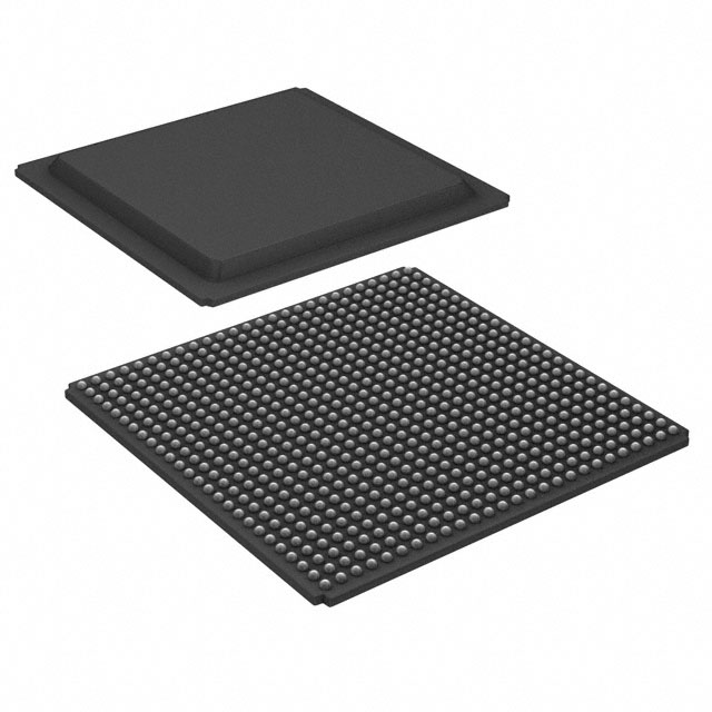
Virtex® Field Programmable Gate Array (FPGA) IC 444 114688 21168 676-BGA |
|---|---|
| Quantity | 112 Available (as of June 15, 2026) |

| Product Category | Field Programmable Gate Array (FPGA) |
|---|---|
| Manufacturer | AMD |
| Manufacturing Status | Obsolete |
| Manufacturer Standard Lead Time | Contact Us |
| Datasheet |
Specifications & Environmental
| Device Package | 676-FBGA (27x27) | Grade | Industrial | Operating Temperature | -40°C – 100°C | ||
|---|---|---|---|---|---|---|---|
| Package / Case | 676-BGA | Number of I/O | 444 | Voltage | 2.375 V - 2.625 V | ||
| Mounting Method | Surface Mount | RoHS Compliance | RoHS non-compliant | REACH Compliance | REACH Unaffected | ||
| Moisture Sensitivity Level | 3 (168 Hours) | Number of LABs/CLBs | 4704 | Number of Logic Elements/Cells | 21168 | ||
| Number of Gates | 888439 | ECCN | 3A991D | HTS Code | 8542.39.0001 | ||
| Qualification | N/A | Total RAM Bits | 114688 |
Overview of XCV800-5FG676I – Virtex FPGA, 21,168 Logic Elements, 676-BGA
The XCV800-5FG676I is an SRAM-based Virtex® Field Programmable Gate Array (FPGA) IC designed for high-capacity, reprogrammable logic applications. It delivers 21,168 logic elements, approximately 0.115 Mbits of embedded memory, and 444 user I/O in a 676-ball FBGA (27×27) package.
Built on the Virtex architecture, this device targets applications that require flexible, high-density programmable logic, on-chip memory configurations, and robust clock management while operating across an industrial temperature range.
Key Features
- Logic Capacity — 21,168 logic elements and 888,439 system gates provide substantial programmable logic resources for complex designs.
- Embedded Memory — Total on-chip RAM of 114,688 bits (approximately 0.115 Mbits) with LUTs and dedicated block RAM that can be configured for various RAM modes.
- High I/O Count — 444 user I/O pins support a wide range of interfacing options and system connectivity.
- SelectIO and Interface Support — Multi-standard SelectIO interfaces with 16 high-performance interface standards for flexible external device connections.
- Clock Management — Four dedicated delay-locked loops (DLLs), four primary low-skew global clock nets and 24 secondary local clock nets for advanced clock control and distribution.
- Dedicated Arithmetic Resources — Built-in carry logic and multiplier support for high-speed arithmetic and DSP-oriented functions.
- SRAM-Based In-System Configuration — Unlimited re-programmability with four programming modes (including SelectMAP, slave serial, master serial and JTAG).
- Process and Test — Implemented in a 0.22 μm 5-layer-metal process and 100% factory tested.
- Industrial Grade & Environmental — Rated for operation from –40°C to 100°C and RoHS compliant.
- Package & Mounting — 676-ball FBGA (27×27) package; surface-mount mounting type; supply voltage 2.375 V to 2.625 V.
Typical Applications
- PCI and CompactPCI Systems — 66-MHz PCI compliance and hot-swappable capability for use in PCI/CompactPCI system designs.
- High-Speed Arithmetic and DSP — Dedicated multiplier and carry logic make the device suitable for compute-heavy signal processing and arithmetic tasks.
- Custom Logic and Prototyping — SRAM-based in-system reconfigurability enables iterative development, prototyping, and field updates.
- Memory-Interfacing Designs — Hierarchical memory architecture and fast external RAM interfaces support systems requiring flexible on-chip and off-chip memory configurations.
Unique Advantages
- High-density Programmability: 21,168 logic elements and 888,439 system gates provide the capacity to integrate complex logic into a single device, reducing board-level component count.
- Flexible On-chip Memory: Approximately 0.115 Mbits of embedded RAM plus LUT-configurable RAM modes allow designers to tailor memory resources to application needs.
- Advanced Clock Control: Four DLLs and an extensive clock-net hierarchy enable precise timing and low-skew distribution for synchronous designs.
- Broad I/O Flexibility: 444 I/O pins and multi-standard SelectIO support simplify interfacing to a variety of peripherals and external memory.
- In-System Reconfigurability: SRAM-based architecture with multiple programming modes supports iterative development and field updates without hardware changes.
- Industrial Reliability: Rated for –40°C to 100°C operation and 100% factory tested to support deployment in industrial environments.
Why Choose XCV800-5FG676I?
The XCV800-5FG676I combines substantial logic density, flexible embedded memory, and advanced clock and I/O features in a single industrial-grade FPGA package. Its Virtex architecture and on-chip resources are suited to engineers building complex, reconfigurable systems that require in-field programmability, robust timing control, and extensive interfacing options.
This device is appropriate for development teams and OEMs seeking a programmable logic solution that supports iterative design workflows, computationally demanding functions, and industrial temperature operation while maintaining a compact, surface-mount footprint.
Request a quote or submit an inquiry to obtain pricing, lead-time, and availability for the XCV800-5FG676I. Our team can provide procurement details and support to help integrate this FPGA into your next design.


Date Founded: 1969
Headquarters: Santa Clara, California, USA
Employees: 25,000+
Revenue: $22.68 Billion
Certifications and Memberships: ISO9001:2015, RoHS, REACH


