
XCV800-5BG560I
| Part Description |
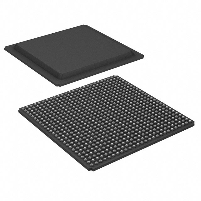
Virtex® Field Programmable Gate Array (FPGA) IC 404 114688 21168 560-LBGA Exposed Pad, Metal |
|---|---|
| Quantity | 249 Available (as of June 18, 2026) |

| Product Category | Field Programmable Gate Array (FPGA) |
|---|---|
| Manufacturer | AMD |
| Manufacturing Status | Obsolete |
| Manufacturer Standard Lead Time | Contact Us |
| Datasheet |
Specifications & Environmental
| Device Package | 560-MBGA (42.5x42.5) | Grade | Industrial | Operating Temperature | -40°C – 100°C | ||
|---|---|---|---|---|---|---|---|
| Package / Case | 560-LBGA Exposed Pad, Metal | Number of I/O | 404 | Voltage | 2.375 V - 2.625 V | ||
| Mounting Method | Surface Mount | RoHS Compliance | RoHS non-compliant | REACH Compliance | REACH Unaffected | ||
| Moisture Sensitivity Level | 3 (168 Hours) | Number of LABs/CLBs | 4704 | Number of Logic Elements/Cells | 21168 | ||
| Number of Gates | 888439 | ECCN | 3A991D | HTS Code | 8542.39.0001 | ||
| Qualification | N/A | Total RAM Bits | 114688 |
Overview of XCV800-5BG560I – Virtex® Field Programmable Gate Array, 560-LBGA
The XCV800-5BG560I is a high-density Virtex® SRAM-based FPGA in a 560-ball LBGA package with exposed pad metal. It combines a large logic fabric with embedded memory and extensive I/O to support complex, reprogrammable system designs in industrial environments.
Built on the Virtex architecture, this device targets applications that require substantial logic capacity, flexible on-chip memory, multi-standard I/O, and reliable clock management while operating across an industrial temperature range.
Key Features
- Logic Capacity — Approximately 21,168 logic elements and 888,439 system gates provide significant on-chip programmable logic for complex designs.
- Embedded Memory — 114,688 total RAM bits (approximately 114.7 Kbits) of on-chip memory with LUTs configurable as various RAM and shift-register modes to support hierarchical memory architectures.
- I/O and Interface Support — 404 user I/O pins with multi-standard SelectIO™ interfaces and fast interfaces to external high-performance RAMs for flexible connectivity.
- Clocking and Timing — Four dedicated delay-locked loops (DLLs), multiple global and local clock distribution nets for advanced clock control and low-skew distribution.
- Configuration and Reprogrammability — SRAM-based in-system configuration with unlimited re-programmability and four programming modes for flexible deployment and updates.
- Package and Thermal — 560-LBGA exposed pad, metal package (560-MBGA, 42.5 × 42.5 mm) designed for surface-mount assembly; specified operating temperature range −40 °C to 100 °C.
- Power and Supply — Supports supply voltage range of 2.375 V to 2.625 V to match board-level power architectures.
- Manufacturing and Process — Implemented in a 0.22 μm, 5-layer metal CMOS process and 100% factory tested; RoHS compliant.
Typical Applications
- PCI and Compact PCI systems — Suitable for designs requiring 66-MHz PCI compliance and hot-swappable Compact PCI capability.
- High-performance system logic — Large logic capacity and dedicated arithmetic resources support compute-intensive custom logic and algorithm acceleration.
- Memory and interface bridging — Configurable LUT RAM and fast external RAM interfaces enable memory-dense functions and protocol bridging to high-performance memories.
- Reconfigurable in-system designs — SRAM-based architecture and unlimited re-programmability allow field updates and iterative development workflows.
Unique Advantages
- High logic density: With roughly 21,168 logic elements and 888,439 system gates, the device supports large, complex designs without immediate external logic.
- Flexible embedded memory: 114,688 bits of RAM and configurable LUT modes provide multiple on-chip memory options for buffering, FIFOs, and local storage.
- Advanced clock management: Four DLLs and hierarchical clock nets enable precise timing control for high-speed synchronous designs.
- Extensive I/O capability: 404 I/O pins and multi-standard SelectIO support simplify interfacing to diverse peripherals and memory devices.
- Industrial temperature range: Rated for −40 °C to 100 °C operation, supporting deployment in temperature-challenging environments.
- Proven silicon and testing: 0.22 μm, 5-layer-metal process with 100% factory testing and RoHS compliance for consistent manufacturing quality.
Why Choose XCV800-5BG560I?
The XCV800-5BG560I is positioned for designs that require a balance of high logic capacity, flexible embedded memory, and robust I/O in a reprogrammable FPGA fabric. Its combination of substantial logic resources, clock-management features, and multi-standard I/O support makes it well-suited for industrial-grade systems that need in-field configurability and reliable operation across a wide temperature range.
For engineering teams building complex, reconfigurable hardware—such as PCI/Compact PCI systems, memory-intensive accelerators, or multi-interface controllers—this device offers a proven architecture and manufacturing pedigree that supports iterative development and long-term deployment.
Request a quote or submit a sales inquiry to obtain pricing, availability, and assistance integrating the XCV800-5BG560I into your next design.


Date Founded: 1969
Headquarters: Santa Clara, California, USA
Employees: 25,000+
Revenue: $22.68 Billion
Certifications and Memberships: ISO9001:2015, RoHS, REACH


