
XCV800-5FG676C
| Part Description |
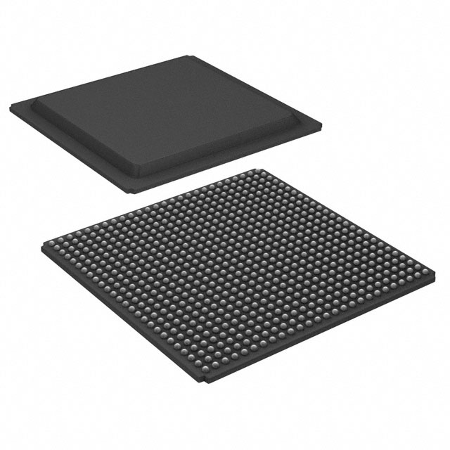
Virtex® Field Programmable Gate Array (FPGA) IC 444 114688 21168 676-BGA |
|---|---|
| Quantity | 727 Available (as of June 15, 2026) |
| Product Category | Field Programmable Gate Array (FPGA) |
|---|---|
| Manufacturer | AMD |
| Manufacturing Status | Obsolete |
| Manufacturer Standard Lead Time | Contact Us |
| Datasheet |
Specifications & Environmental
| Device Package | 676-FBGA (27x27) | Grade | Commercial | Operating Temperature | 0°C – 85°C | ||
|---|---|---|---|---|---|---|---|
| Package / Case | 676-BGA | Number of I/O | 444 | Voltage | 2.375 V - 2.625 V | ||
| Mounting Method | Surface Mount | RoHS Compliance | RoHS non-compliant | REACH Compliance | REACH Unaffected | ||
| Moisture Sensitivity Level | 3 (168 Hours) | Number of LABs/CLBs | 4704 | Number of Logic Elements/Cells | 21168 | ||
| Number of Gates | 888439 | ECCN | 3A991D | HTS Code | 8542.39.0001 | ||
| Qualification | N/A | Total RAM Bits | 114688 |
Overview of XCV800-5FG676C – Virtex FPGA, 21,168 logic elements, 676‑BGA
The XCV800-5FG676C is a high-density Virtex® Field Programmable Gate Array (FPGA) in a 676-ball BGA package, delivering 21,168 logic elements and approximately 0.115 Mbits of embedded block RAM. It is an SRAM-based, reprogrammable FPGA designed for system designs that require substantial programmable logic, abundant I/O, and integrated memory and clock-management resources.
This device targets high-performance programmable logic applications where on-chip integration of logic, memory, and multi-standard I/O reduces system complexity and accelerates time-to-market.
Key Features
- Logic Capacity — 21,168 logic elements and 888,439 system gates provide substantial on-chip programmable logic density for complex designs.
- Embedded Memory — Approximately 0.115 Mbits (114,688 bits) of block RAM for implementing data buffers, FIFOs, and small on-chip memory structures.
- I/O Density — 444 user I/O pins to support wide parallel interfaces and multiple external peripherals.
- Clock Management — Four dedicated delay-locked loops (DLLs), four primary low-skew global clock nets and 24 secondary local clock nets for flexible, low-skew clock distribution.
- Configurable Logic — LUTs configurable as RAM (16/32-bit), dual-ported RAM, or shift registers; dedicated carry logic and multiplier support for arithmetic-intensive functions.
- In-System Reprogrammability — SRAM-based configuration with multiple programming modes for unlimited re-programmability and iterative development.
- Package & Mounting — 676‑FBGA (27×27) surface-mount package (676‑BGA) for compact board-level integration.
- Power and Operating Range — Core supply 2.375 V to 2.625 V; commercial operating temperature range 0 °C to 85 °C.
- Compliance — RoHS compliant.
Typical Applications
- PCI and CompactPCI systems — Supports PCI-compliant interfaces and hot-swappable CompactPCI applications requiring programmable logic and high I/O counts.
- High-performance embedded systems — On-chip memory, clock management and arithmetic resources for signal processing and control tasks.
- Custom interface bridging — Extensive I/O and multi-standard SelectIO capability for bridging between different bus and memory standards.
Unique Advantages
- High on-chip integration: Combines 21,168 logic elements and embedded block RAM to reduce external component count and simplify BOM.
- Flexible clocking: Multiple DLLs and hierarchical clock nets enable precise timing control across large designs.
- Extensive I/O capacity: 444 I/O pins support wide parallel buses and multiple peripheral interfaces without external expanders.
- Reconfigurable development flow: SRAM-based, in-system configuration allows iterative prototyping and field updates.
- Compact board footprint: 676‑FBGA (27×27) surface-mount package supports dense PCB layouts while keeping high pin-count accessibility.
- Standards-oriented features: Built-in support for multi-standard I/O and memory interfacing to streamline system-level integration.
Why Choose XCV800-5FG676C?
The XCV800-5FG676C provides a balance of logic density, embedded memory, and extensive I/O in a compact 676‑BGA package, suited to engineers building high-performance programmable solutions. With dedicated clock-management resources and reprogrammable SRAM configuration, it supports iterative development and flexible deployment models.
This device is appropriate for design teams seeking a robust, field-programmable logic element with clear electrical and environmental specifications (2.375–2.625 V core supply, 0 °C to 85 °C operating range) and RoHS compliance for modern electronic assemblies.
Request a quote or submit a product inquiry to receive pricing, availability, and additional technical support for the XCV800-5FG676C.


Date Founded: 1969
Headquarters: Santa Clara, California, USA
Employees: 25,000+
Revenue: $22.68 Billion
Certifications and Memberships: ISO9001:2015, RoHS, REACH


