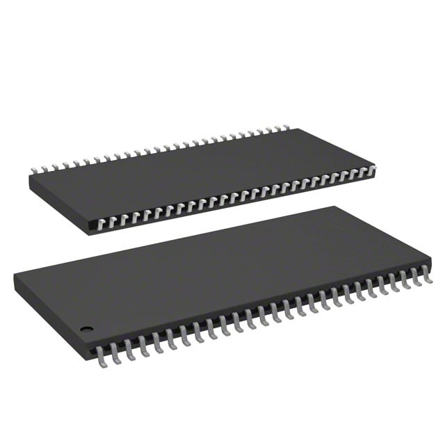
IS42S83200D-7TL-TR
| Part Description |
IC DRAM 256MBIT PAR 54TSOP II |
|---|---|
| Quantity | 27 Available (as of June 9, 2026) |

| Product Category | Memory |
|---|---|
| Manufacturer | Integrated Silicon Solution Inc |
| Manufacturing Status | Obsolete |
| Manufacturer Standard Lead Time | Contact Us |
| Datasheet |
Specifications & Environmental
| Device Package | 54-TSOP II | Memory Format | DRAM | Technology | SDRAM | ||
|---|---|---|---|---|---|---|---|
| Memory Size | 256 Mbit | Access Time | 5.4 ns | Grade | Commercial | ||
| Clock Frequency | 143 MHz | Voltage | 3V ~ 3.6V | Memory Type | Volatile | ||
| Operating Temperature | 0°C ~ 70°C (TA) | Write Cycle Time Word Page | N/A | Packaging | 54-TSOP (0.400", 10.16mm Width) | ||
| Mounting Method | Volatile | Memory Interface | Parallel | Memory Organization | 32M x 8 | ||
| Moisture Sensitivity Level | 3 (168 Hours) | RoHS Compliance | ROHS3 Compliant | REACH Compliance | REACH Unaffected | ||
| Qualification | N/A | ECCN | EAR99 | HTS Code | 8542.32.0024 |
Overview of IS42S83200D-7TL-TR – IC DRAM 256MBIT PAR 54TSOP II
The IS42S83200D-7TL-TR is a 256‑Mbit synchronous DRAM (SDRAM) organized as 32M × 8, implementing a pipelined architecture for high-speed data transfer. It is a fully synchronous, parallel memory device with internal bank management designed for systems that require predictable, clock‑edge referenced memory operations.
Targeted at designs requiring a commercial temperature range and compact package footprint, this SDRAM delivers programmable burst operation, selectable CAS latency, and standard LVTTL signaling for parallel memory interfaces.
Key Features
- Memory Organization 256 Mbit total, organized as 32M × 8 (8M × 8 × 4 banks) to support multi‑bank operation and hidden row access/precharge.
- Synchronous Pipeline Architecture Fully synchronous operation with all signals referenced to the rising edge of the clock for deterministic timing.
- Clock & Timing Supports clock frequency up to 143 MHz (‑7 speed grade) with programmable CAS latency (2 or 3 clocks) and an access time from clock of 5.4 ns (CL = 3).
- Burst and Access Modes Programmable burst lengths (1, 2, 4, 8, full page) and burst sequence (Sequential/Interleave); supports burst read/write and burst read/single write operations with burst termination commands.
- Refresh & Retention Auto Refresh (CBR) and Self Refresh supported; 8K refresh cycles with selectable interval behavior (e.g., 8K/16 ms for A2 grade or 8K/64 ms for commercial/industrial/A1 grade as specified).
- Interface & Logic Levels LVTTL interface compatible with parallel memory systems.
- Power Single power supply: 3.3 V ±0.3 V (specified supply range 3.0 V to 3.6 V).
- Package 54‑pin TSOP‑II (0.400", 10.16 mm width) surface mount package for dense board integration.
- Operating Temperature Commercial ambient range specified as 0 °C to +70 °C (TA).
Typical Applications
- Embedded memory subsystems Parallel SDRAM for systems that require synchronous, banked memory with programmable burst operation.
- High‑throughput buffering Use as a high‑speed buffer memory where pipelined read/write transfers and selectable CAS latency improve throughput determinism.
- Consumer and commercial electronics Memory resource for devices operating in a 0 °C to +70 °C ambient range that require standard LVTTL parallel SDRAM interfaces.
Unique Advantages
- High‑speed, predictable timing: Clocked SDRAM operation and pipeline architecture enable high‑speed data transfer with timing referenced to the rising clock edge.
- Flexible performance tuning: Programmable burst lengths, burst sequencing, and selectable CAS latency (2 or 3 clocks) let designers balance latency and throughput.
- Single‑supply simplicity: 3.3 V ±0.3 V single supply (3.0–3.6 V) simplifies power rail requirements for many system designs.
- On‑chip refresh management: Auto Refresh and Self Refresh support with 8K refresh cycles provide standard DRAM retention control without external intervention.
- Compact board footprint: 54‑pin TSOP‑II package (0.400", 10.16 mm width) enables dense memory placement on space‑constrained PCBs.
- Standard LVTTL interface: Compatibility with common parallel logic levels eases integration into existing memory controller designs.
Why Choose IS42S83200D-7TL-TR?
The IS42S83200D-7TL-TR positions itself as a reliable 256‑Mbit parallel SDRAM option for commercial temperature systems that need clocked, banked memory with programmable performance characteristics. Its pipelined synchronous architecture, selectable CAS latency, and multiple burst modes provide designers with the timing control required for predictable, high‑speed data transfers.
Suitable for embedded and consumer/commercial applications that require a compact 54‑pin TSOP‑II package and a single 3.3 V supply, this device offers standard refresh and self‑refresh features and LVTTL signaling for straightforward integration into parallel memory subsystems.
Request a quote or submit an inquiry to receive pricing and availability for the IS42S83200D-7TL-TR for your next design.