IS42S83200D-7TL
| Part Description |
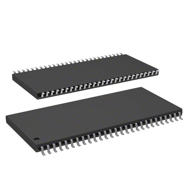
IC DRAM 256MBIT PAR 54TSOP II |
|---|---|
| Quantity | 1,123 Available (as of June 10, 2026) |

| Product Category | Memory |
|---|---|
| Manufacturer | Integrated Silicon Solution Inc |
| Manufacturing Status | Obsolete |
| Manufacturer Standard Lead Time | Contact Us |
| Datasheet |
Specifications & Environmental
| Device Package | 54-TSOP II | Memory Format | DRAM | Technology | SDRAM | ||
|---|---|---|---|---|---|---|---|
| Memory Size | 256 Mbit | Access Time | 5.4 ns | Grade | Commercial | ||
| Clock Frequency | 143 MHz | Voltage | 3V ~ 3.6V | Memory Type | Volatile | ||
| Operating Temperature | 0°C ~ 70°C (TA) | Write Cycle Time Word Page | N/A | Packaging | 54-TSOP (0.400", 10.16mm Width) | ||
| Mounting Method | Volatile | Memory Interface | Parallel | Memory Organization | 32M x 8 | ||
| Moisture Sensitivity Level | 3 (168 Hours) | RoHS Compliance | ROHS3 Compliant | REACH Compliance | REACH Unaffected | ||
| Qualification | N/A | ECCN | EAR99 | HTS Code | 8542.32.0024 |
Overview of IS42S83200D-7TL – IC DRAM 256MBIT PAR 54TSOP II
The IS42S83200D-7TL is a 256‑Mbit synchronous DRAM (SDRAM) organized as 32M × 8 with four internal banks and a parallel LVTTL interface. It uses a pipelined, fully synchronous architecture referenced to the rising clock edge to support high‑speed data transfer.
This device targets commercial‑temperature applications and provides programmable burst modes, selectable CAS latency, auto/self refresh, and single‑supply 3.3V operation to support designs that require compact, parallel SDRAM memory.
Key Features
- Core / Architecture Fully synchronous SDRAM with pipelined architecture; all signals referenced to the positive clock edge and internal bank structure to hide row access/precharge.
- Memory Density & Organization 256 Mbit capacity organized as 32M × 8 with 4 banks, providing parallel DRAM storage in a single device.
- Programmable Burst & Access Programmable burst lengths (1, 2, 4, 8, full page) and burst sequence selection (Sequential/Interleave); supports burst read/write and burst read/single write operations.
- Timing & Performance Specified for 143 MHz operation (–7 speed grade) with CAS latency options (2 or 3 clocks) and an access time from clock of 5.4 ns at CL=3.
- Power Single power supply: 3.3 V ± 0.3 V (operating range 3.0 V to 3.6 V) for straightforward power rail design.
- Refresh & Retention Auto Refresh (CBR) and Self Refresh supported; refresh options include 8K refresh cycles with 64 ms (commercial/A1) and 16 ms (A2) intervals as specified.
- Interface LVTTL compatible signals and parallel memory interface for integration into synchronous memory subsystems.
- Package & Temperature 54‑pin TSOP II package (0.400", 10.16 mm width) with an operating temperature range of 0°C to 70°C (TA).
Typical Applications
- Systems requiring synchronous DRAM Use where a fully synchronous, pipelined DRAM is required for parallel memory access and predictable timing.
- Commercial electronic products Suitable for designs operating within 0°C to 70°C that need 256 Mbit of parallel SDRAM capacity in a compact TSOP II package.
- High‑speed burst data paths Designed for applications that leverage programmable burst length and sequence to optimize sustained transfer efficiency.
Unique Advantages
- Predictable, synchronous timing: Programmable CAS latency (2 or 3 clocks) and clock‑edge referenced operation enable consistent timing behavior in synchronous memory subsystems.
- Flexible burst control: Programmable burst lengths and sequence options allow designers to tune throughput for sequential or interleaved access patterns.
- High read performance at –7 grade: 143 MHz clock rate with a 5.4 ns access time (CL=3) supports fast cycle‑to‑cycle data transfers.
- Simple power integration: Single‑supply 3.3 V ±0.3 V operation (3.0–3.6 V) reduces supply complexity for memory rails.
- Space‑efficient packaging: 54‑pin TSOP II (10.16 mm width) provides a compact footprint for space‑constrained PCB layouts.
- Built‑in refresh modes: Auto and self‑refresh support with specified 8K refresh cycles permit reliable data retention across different refresh interval options.
Why Choose IS42S83200D-7TL?
The IS42S83200D-7TL combines a 256‑Mbit SDRAM density with a fully synchronous, pipelined architecture and programmable timing features to deliver predictable performance in commercial‑temperature systems. Its selectable CAS latency, programmable burst modes, and LVTTL interface make it suitable for designs that require controlled, parallel SDRAM behavior in a compact TSOP II package.
Manufactured by Integrated Silicon Solution, Inc., the device provides a clear specification set—clocking, access timing, power, refresh options, and package details—allowing engineers to evaluate fit for memory subsystems where 3.3V single‑supply operation and 0°C to 70°C commercial operation are required.
Request a quote or submit a sales inquiry to obtain pricing, availability, and lead‑time information for the IS42S83200D-7TL.