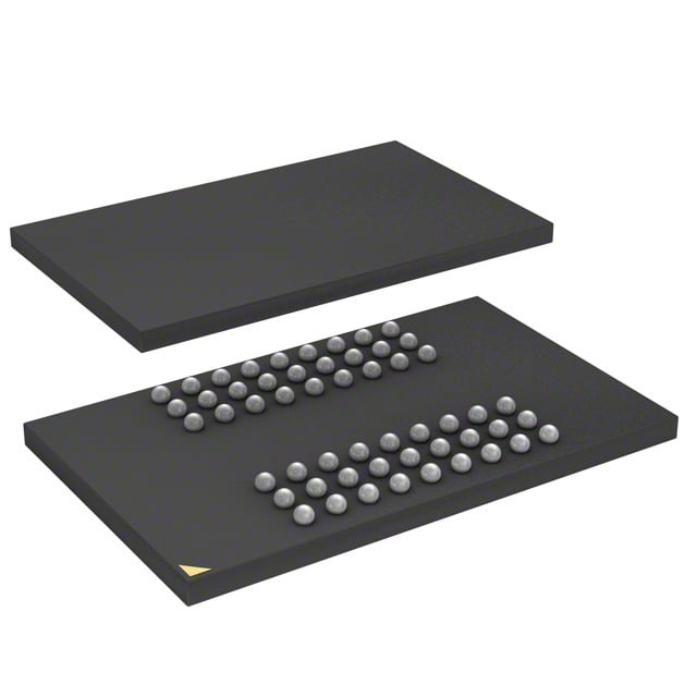
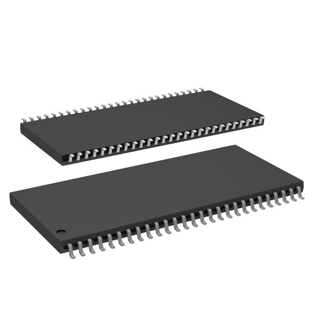
IS45S16320D-6CTLA1
| Part Description |
IC DRAM 512MBIT PAR 54TSOP II |
|---|---|
| Quantity | 31 Available (as of June 9, 2026) |

| Product Category | Memory |
|---|---|
| Manufacturer | Integrated Silicon Solution Inc |
| Manufacturing Status | Obsolete |
| Manufacturer Standard Lead Time | Contact Us |
| Datasheet |
Specifications & Environmental
| Device Package | 54-TSOP II | Memory Format | DRAM | Technology | SDRAM | ||
|---|---|---|---|---|---|---|---|
| Memory Size | 512 Mbit | Access Time | 5.4 ns | Grade | Industrial | ||
| Clock Frequency | 166 MHz | Voltage | 3V ~ 3.6V | Memory Type | Volatile | ||
| Operating Temperature | -40°C ~ 85°C (TA) | Write Cycle Time Word Page | N/A | Packaging | 54-TSOP (0.400", 10.16mm Width) | ||
| Mounting Method | Volatile | Memory Interface | Parallel | Memory Organization | 32M x 16 | ||
| Moisture Sensitivity Level | 3 (168 Hours) | RoHS Compliance | ROHS3 Compliant | REACH Compliance | REACH Unaffected | ||
| Qualification | N/A | ECCN | EAR99 | HTS Code | 8542.32.0032 |
Overview of IS45S16320D-6CTLA1 – IC DRAM 512MBIT PAR 54TSOP II
The IS45S16320D-6CTLA1 is a 512 Mbit synchronous DRAM (SDRAM) organized as 32M × 16 with a parallel memory interface. It uses a pipeline architecture and fully synchronous timing referenced to the rising edge of the clock to enable high-speed data transfer.
Designed for applications requiring a 512 Mbit SDRAM with programmable burst control and internal bank management, this device delivers deterministic access characteristics and supports operation across an extended temperature range.
Key Features
- Memory Organization and Capacity — 512 Mbit total capacity arranged as 32M × 16, providing a wide parallel data path for high-throughput systems.
- Synchronous Pipeline Architecture — Fully synchronous operation with all signals referenced to the positive clock edge; internal bank structure hides row access/precharge to improve effective throughput.
- Performance — Rated clock frequency for this device is 166 MHz with an access time from clock of 5.4 ns (CAS latency = 3 at -6 speed grade).
- Programmable Burst and CAS — Supports programmable burst lengths (1, 2, 4, 8, full page) and selectable burst sequence (sequential/interleave); programmable CAS latency of 2 or 3 clocks.
- Refresh and Power Management — Auto-Refresh and Self-Refresh supported with 8K refresh cycles per 64 ms for standard operation.
- Interface and Signaling — Parallel memory interface with LVTTL-compatible signaling.
- Voltage Range — Operational supply range of 3.0 V to 3.6 V.
- Package — Supplied in a 54-pin TSOP-II package (0.400", 10.16 mm width) suitable for compact board-level designs.
- Operating Temperature — Rated for operation from −40°C to +85°C (TA).
Typical Applications
- System Memory Expansion — Use as a 512 Mbit SDRAM in systems requiring parallel DRAM memory for high-throughput data buffering and storage.
- High-Speed Data Buffers — Suitable for applications that benefit from synchronous pipeline operation and internal bank management to improve sustained data transfer.
- Industrial-Temperature Designs — Applicable in designs that require memory operation across −40°C to +85°C ambient temperatures.
Unique Advantages
- Deterministic Synchronous Timing: Fully synchronous clock-referenced operation simplifies timing analysis and system integration.
- Flexible Burst Control: Programmable burst lengths and sequence options allow tuning for sequential or random access patterns.
- Internal Bank Architecture: Banked memory hides row access/precharge cycles to improve effective throughput for burst operations.
- Compact TSOP-II Package: 54-pin TSOP-II footprint provides a space-efficient solution for board-level memory implementations.
- Extended Temperature Range: Rated for −40°C to +85°C to support applications operating across a wide ambient temperature window.
- Wide Supply Tolerance: Operates from 3.0 V to 3.6 V to accommodate common 3.3 V system power rails.
Why Choose IS45S16320D-6CTLA1?
The IS45S16320D-6CTLA1 combines 512 Mbit capacity with a 32M × 16 organization and a synchronous pipeline architecture to provide predictable, high-speed parallel DRAM performance. Its programmable burst modes, CAS options, and internal bank management make it suitable for designs that require configurable throughput and efficient burst handling.
With a 54-pin TSOP-II package, support for standard LVTTL signaling, a 3.0–3.6 V supply window, and operation from −40°C to +85°C, this device is aimed at engineers implementing compact, robust memory subsystems backed by Integrated Silicon Solution, Inc.'s product specification and documentation.
If you need pricing, availability or to request a quote for the IS45S16320D-6CTLA1, please contact sales to discuss lead times and ordering details.