MT53E1G64D4HJ-046 WT:C
| Part Description |
IC DRAM 64GBIT PAR 556WFBGA |
|---|---|
| Quantity | 1,384 Available (as of June 9, 2026) |

| Product Category | Memory |
|---|---|
| Manufacturer | Micron Technology Inc. |
| Manufacturing Status | Active |
| Manufacturer Standard Lead Time | 39 Weeks |
| Datasheet |
Specifications & Environmental
| Device Package | 556-WFBGA (12.4x12.4) | Memory Format | DRAM | Technology | SDRAM - Mobile LPDDR4X | ||
|---|---|---|---|---|---|---|---|
| Memory Size | 64 Gbit | Access Time | 3.5 ns | Grade | Industrial | ||
| Clock Frequency | 2.133 GHz | Voltage | 1.06V ~ 1.17V | Memory Type | Volatile | ||
| Operating Temperature | -30°C ~ 85°C (TC) | Write Cycle Time Word Page | 18 ns | Packaging | 556-TFBGA | ||
| Mounting Method | Volatile | Memory Interface | Parallel | Memory Organization | 1G x 64 | ||
| Moisture Sensitivity Level | 3 (168 Hours) | RoHS Compliance | ROHS3 Compliant | REACH Compliance | REACH Unaffected | ||
| Qualification | N/A | ECCN | EAR99 | HTS Code | 8542.32.0036 |
Overview of MT53E1G64D4HJ-046 WT:C – IC DRAM 64Gbit PAR 556WFBGA
The MT53E1G64D4HJ-046 WT:C is a 64 Gbit volatile DRAM device implemented as a 1G x 64 LPDDR4X/LPDDR4 SDRAM. It provides a parallel memory interface in a 556-ball W/TFBGA package (12.4 × 12.4 mm) and is targeted at systems using mobile LPDDR4X architecture.
Designed for high-speed, low-voltage operation, this device supports a 2.133 GHz clock (4266 Mb/s data rate per pin) and offers features intended to simplify high-bandwidth memory subsystem design while providing thermal and refresh controls for efficient operation.
Key Features
- Core and I/O power — Ultra-low-voltage supply options with VDD2 = 1.06–1.17 V and selectable VDDQ (0.57–0.65 V or 1.06–1.17 V) to support low-power system designs.
- Performance — 2.133 GHz clock frequency with a data rate per pin of 4266 Mb/s and a 16n prefetch DDR architecture for high-throughput memory access.
- Memory organization — 1G × 64 array configuration (64 Gbit total) with 8 internal banks per channel for concurrent bank operation.
- Timing — Write cycle time (word page) of 18 ns and documented access timing (read/write latencies programmable; RL/WL), with example speed-grade timing at -046.
- Power and thermal management — On-chip temperature sensor to control self-refresh rate and partial-array self refresh (PASR) for targeted power savings.
- Refresh and command features — Directed per-bank refresh for concurrent bank operation and single-data-rate CMD/ADR entry for command sequencing.
- Data integrity and IO control — Programmable DBI options, selectable output drive strength (DS), programmable VSS (ODT) termination, and bidirectional/differential data strobe per byte lane.
- Burst and latency programmability — Programmable on-the-fly burst lengths (BL = 16, 32) and programmable READ and WRITE latencies to match system timing requirements.
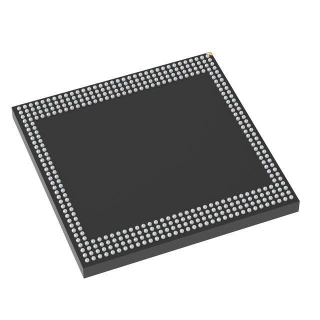
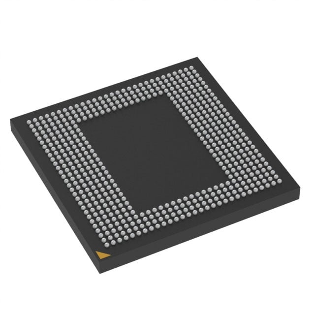
- Package and mounting — 556-ball TFBGA / WFBGA package (12.4 × 12.4 mm) suitable for compact board layouts; supplier device package listed as 556-WFBGA (12.4 × 12.4).
- Operating range — Documented operating temperature from -30°C to +85°C (TC) and supply voltage range VDD2 = 1.06–1.17 V.
Typical Applications
- Mobile memory subsystems — LPDDR4X configuration and low-voltage supplies make the device appropriate for mobile-oriented memory channels requiring high data rates.
- High-bandwidth embedded systems — 2.133 GHz clock and 4266 Mb/s per-pin data rate support systems that need sustained memory throughput.
- Compact board designs — 556-ball W/TFBGA 12.4 × 12.4 mm package for space-constrained layouts where a 64 Gbit die density is required.
Unique Advantages
- Low-voltage operation: VDD2 and VDDQ supply options reduce core and I/O power consumption compared to higher-voltage DRAM alternatives, aiding energy-sensitive designs.
- High data-rate capability: 4266 Mb/s per pin (2.133 GHz clock) enables high-throughput memory channels for bandwidth-intensive tasks.
- Flexible timing and burst control: Programmable RL/WL and selectable burst lengths (BL = 16, 32) allow designers to tune performance to system timing and workload.
- Banked refresh and thermal management: Directed per-bank refresh and on-chip temperature sensing provide options to optimize refresh scheduling and self-refresh behavior for power and performance balance.
- Dense, compact packaging: 556-ball TFBGA/WFBGA package (12.4 × 12.4 mm) delivers 64 Gbit capacity in a small footprint for space-constrained PCBs.
Why Choose MT53E1G64D4HJ-046 WT:C?
The MT53E1G64D4HJ-046 WT:C combines LPDDR4X/LPDDR4 architecture, low-voltage supply options, and a high data-rate interface to provide a compact, high-density DRAM solution for designs that require both throughput and power efficiency. Its programmable latencies, burst lengths, per-bank refresh capability, and on-chip thermal sensing give system designers the control needed to tune memory behavior to application needs.
This device is well suited for engineers specifying mobile LPDDR4X memory subsystems, compact board layouts, or designs requiring 64 Gbit density with documented timing and supply ranges. The package and electrical characteristics support integration into dense, performance-oriented memory architectures.
Request a quote or submit an inquiry to receive pricing and availability details for the MT53E1G64D4HJ-046 WT:C.