W9425G6JB-5I TR
| Part Description |
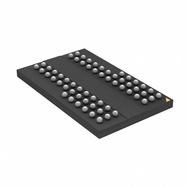
IC DRAM 256MBIT PAR 60TFBGA |
|---|---|
| Quantity | 1,373 Available (as of June 9, 2026) |

| Product Category | Memory |
|---|---|
| Manufacturer | Winbond Electronics |
| Manufacturing Status | Obsolete |
| Manufacturer Standard Lead Time | Contact Us |
| Datasheet |
Specifications & Environmental
| Device Package | 60-TFBGA (8x13) | Memory Format | DRAM | Technology | SDRAM - DDR | ||
|---|---|---|---|---|---|---|---|
| Memory Size | 256 Mbit | Access Time | 55 ns | Grade | Industrial | ||
| Clock Frequency | 200 MHz | Voltage | 2.3V ~ 2.7V | Memory Type | Volatile | ||
| Operating Temperature | -40°C ~ 85°C (TA) | Write Cycle Time Word Page | 15 ns | Packaging | 60-TFBGA | ||
| Mounting Method | Volatile | Memory Interface | Parallel | Memory Organization | 16M x 16 | ||
| Moisture Sensitivity Level | 3 (168 Hours) | RoHS Compliance | ROHS Compliant | REACH Compliance | REACH Unaffected | ||
| Qualification | N/A | ECCN | EAR99 | HTS Code | 8542.32.0002 |
Overview of W9425G6JB-5I TR – IC DRAM 256MBIT PAR 60TFBGA
The W9425G6JB-5I TR is a 256 Mbit DDR SDRAM device organized as 16M × 16 (4 M × 4 banks × 16 bits) with a parallel memory interface. It implements DDR SDRAM architecture with documented command sequences and timing, delivered in a 60-TFBGA (8×13) package.
Key electrical and timing characteristics include a 200 MHz clock frequency, 55 ns access time, a 15 ns write cycle time for word page operations, and a supply voltage range of 2.3 V to 2.7 V. The device is specified for operation from -40°C to 85°C (TA).
Key Features
- Memory Type & Capacity — 256 Mbit DRAM implemented as 16M × 16, arranged in 4 banks × 4 M × 4 configuration.
- DDR Architecture — DDR SDRAM with documented command functions (Bank Activate, Read/Write, Auto Refresh, Self Refresh, Mode Register Set and Extended Mode Register Set) and timing waveforms.
- Performance — 200 MHz clock frequency with a specified access time of 55 ns and a write cycle time (word page) of 15 ns.
- Voltage — Recommended supply voltage range from 2.3 V to 2.7 V.
- Package — 60-TFBGA (8×13) BGA package to minimize board footprint.
- Temperature Range — Rated for operation from -40°C to 85°C (TA).
- Timing & Mode Control — Mode register and extended mode register fields include burst length, addressing mode, CAS latency, and DLL reset as specified in the datasheet.
Unique Advantages
- Compact BGA footprint: 60-TFBGA (8×13) package reduces PCB area for space-constrained layouts.
- DDR operation at 200 MHz: Synchronous read/write bursts supported with full timing and command documentation for system integration.
- Flexible power domain design: 2.3–2.7 V supply range allows compatibility with a range of system power architectures.
- Extended temperature rating: -40°C to 85°C (TA) supports industrial temperature environments.
- Comprehensive datasheet detail: Power-up sequence, command set, timing waveforms, and system characteristic tables are provided for design validation and integration.
Why Choose IC DRAM 256MBIT PAR 60TFBGA?
The W9425G6JB-5I TR delivers a 256 Mbit DDR SDRAM option with clear electrical and timing specifications, compact 60-TFBGA packaging, and an extended operating temperature range. Its documented command set and timing tables simplify integration into systems that require parallel DDR memory and deterministic timing behavior.
This device is suited to designs that need a 256 Mbit DDR memory element with a small BGA footprint and defined supply and timing ranges. The availability of detailed datasheet information supports validation, sequencing, and timing verification during development.
Request a quote or contact sales to submit requirements and receive pricing and availability information for the W9425G6JB-5I TR.