
MCIMX7S5EVK08SC
| Part Description |
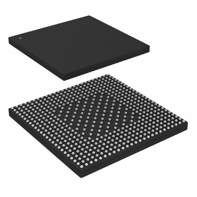
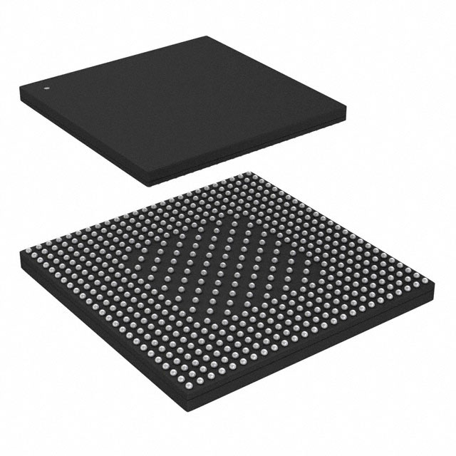
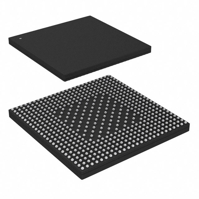
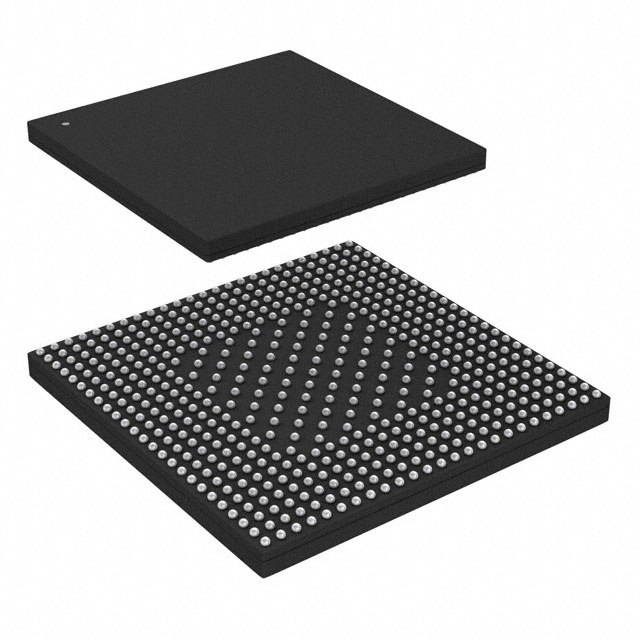
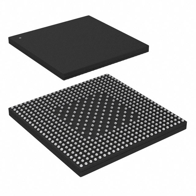
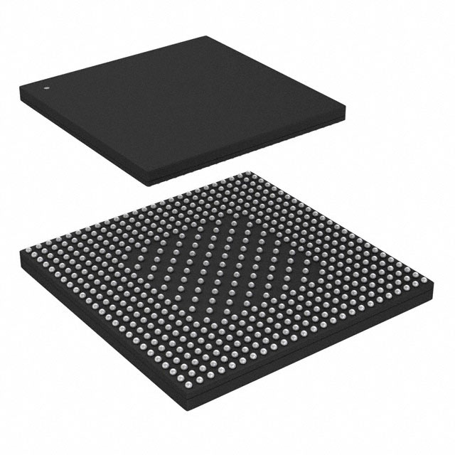
ARM® Cortex®-A7, ARM® Cortex®-M4 Microprocessor IC i.MX7S 1 Core, 32-Bit 800MHz 488-TFBGA (12x12) |
|---|---|
| Quantity | 716 Available (as of October 8, 2026) |

| Product Category | Microprocessors |
|---|---|
| Part Series | i.MX 7S |
| Manufacturer | NXP USA Inc. |
| Manufacturing Status | Active |
| Manufacturer Standard Lead Time | 0 Weeks |
| Datasheet |
Specifications & Environmental
| Co-Processors/DSP | Multimedia; NEON™ MPE | Core Processor | ARM® Cortex®-A7, ARM® Cortex®-M4 | Device Package | 488-TFBGA (12x12) | ||
|---|---|---|---|---|---|---|---|
| Display & Interface Controllers | Keypad, LCD, MIPI | ECCN | 5A992C | Ethernet | 10/100/1000Mbps (1) | ||
| Graphics Acceleration | No | HTS Code | 8542.31.0001 | Moisture Sensitivity Level | N/A | ||
| Mounting Method | Surface Mount | Mounting Type | Surface Mount | Number of Cores/Bus Width | 1 Core, 32-Bit | ||
| Operating Temperature | -20°C ~ 105°C (TJ) | Package / Case | 488-TFBGA | RAM Controllers | LPDDR2, LPDDR3, DDR3, DDR3L | ||
| REACH Compliance | REACH Unknown | RoHS Compliance | Unknown | Security Features | A-HAB, ARM TZ, CAAM, CSU, SJC, SNVS | ||
| Speed | 800MHz | Supplier Device Package | 488-TFBGA (12×12) | USB | USB 2.0 + PHY (1), USB 2.0 OTG + PHY (1) | ||
| Voltage – I/O | 1.8V, 3.3V |
Overview of MCIMX7S5EVK08SC – IC MPU I.MX7S 800MHZ 488TFBGA
The MCIMX7S5EVK08SC is an i.MX 7S microprocessor IC featuring ARM® Cortex®-A7 and ARM® Cortex®-M4 processor architectures with a 32-bit core and an 800 MHz operating frequency. Designed for embedded applications, this device provides a balance of processing capability and system integration for connected and secure embedded designs.
With on-chip support for multiple memory types, a range of system interfaces and hardware security modules, the part targets embedded systems that require integrated connectivity, flexible memory options and hardware-based security features.
Key Features
- Core Architecture – ARM® Cortex®-A7 and ARM® Cortex®-M4 processors listed as the core processing engines; device specified as 1 Core, 32‑Bit running at 800 MHz.
- Memory Interfaces – Supported RAM controllers include LPDDR2, LPDDR3, DDR3 and DDR3L, allowing flexible memory choices for system designers.
- Connectivity – Integrated 10/100/1000 Mbps Ethernet (1) and USB 2.0 + PHY (1) plus USB 2.0 OTG + PHY (1) provide wired networking and host/device USB connectivity options.
- Display and I/O – Display interface controllers include keypad, LCD and MIPI, enabling user interface and display integration.
- Security Subsystem – Hardware security features include A-HAB, ARM TrustZone (ARM TZ), CAAM, CSU, SJC and SNVS to support protected boot and system-level security functions.
- Co-Processing – Multimedia co-processor support and NEON™ MPE acceleration are indicated for media and signal processing tasks.
- Package and Mounting – Supplied in a 488‑TFBGA package (12×12) with surface mount mounting suitable for compact PCB designs.
- Operating Range – Specified operating temperature range from −20 °C to 105 °C for deployment across a range of embedded environments.
- Additional Interfaces – AC'97 interface supported for legacy audio connectivity.
- Environmental Compliance – RoHS compliant.
- Graphics Acceleration – No graphics acceleration is specified for this device.
Typical Applications
- Embedded Control Systems – Use the on-chip processing and multiple memory controller options to implement control and management functions in embedded products.
- Networking and Gateway Devices – Integrated Gigabit Ethernet and USB interfaces support wired connectivity for gateway and connected device applications.
- Human-Machine Interfaces (HMI) – LCD and MIPI display interface controllers with keypad support enable development of user interface solutions.
- Secure Embedded Platforms – Hardware security modules (A-HAB, ARM TZ, CAAM, CSU, SJC, SNVS) provide the foundation for secure boot and system-level protection.
Unique Advantages
- Flexible Memory Support: Multiple RAM controller options (LPDDR2, LPDDR3, DDR3, DDR3L) let designers choose memory configurations that match performance and cost targets.
- Integrated Connectivity: Built-in Gigabit Ethernet and USB 2.0 host/OTG PHYs reduce the need for external controllers and simplify board-level integration.
- On-chip Security Features: Comprehensive hardware security building blocks support secure boot and trusted execution models, helping to harden devices against software attack vectors.
- Compact Package: The 488‑TFBGA (12×12) surface-mount package supports compact PCB designs where board space is constrained.
- Broad Operating Range: Rated for −20 °C to 105 °C operation, enabling use in a variety of embedded environments.
Why Choose MCIMX7S5EVK08SC?
The MCIMX7S5EVK08SC combines ARM Cortex processing architectures with broad memory interface support, integrated wired connectivity and a suite of hardware security features to deliver a well-rounded microprocessor solution for embedded designs. Its 488‑TFBGA package and specified temperature range make it suitable for compact, robust systems where integration and security are priorities.
This part is suited to engineers and procurement teams building connected embedded products that require flexible memory options, Ethernet and USB connectivity, and hardware-based security primitives while maintaining a compact board footprint.
Request a quote or submit a product inquiry to receive pricing and availability for the MCIMX7S5EVK08SC.



















Date Founded: 2006
Headquarters: Eindhoven, North Brabant, Netherlands
Employees: 38,000+
Revenue: $10.53 Billion
Certifications and Memberships: ISO9001:2015, IATF16949:2016


