
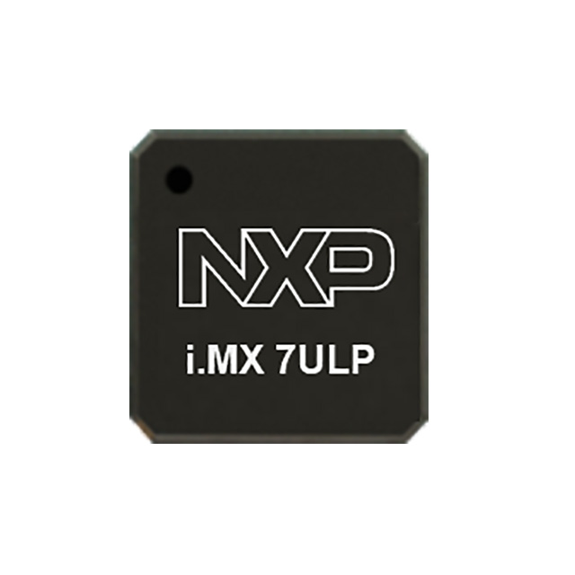
MCIMX7U3CVP06SD
| Part Description |
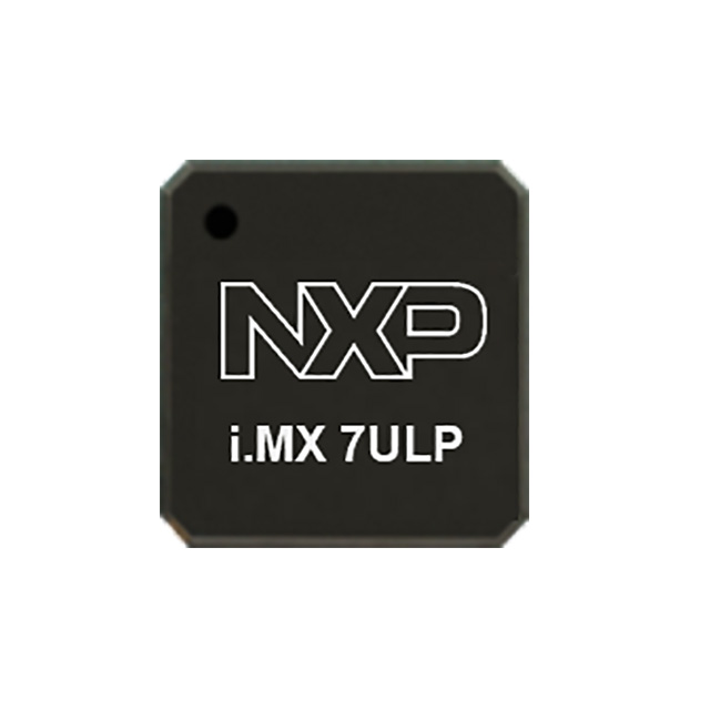
IC I.MX 7ULP MAPBGA 393 |
|---|---|
| Quantity | 481 Available (as of October 8, 2026) |
| Product Category | Microprocessors |
|---|---|
| Part Series | i.MX 7U |
| Manufacturer | NXP USA Inc. |
| Manufacturing Status | Active |
| Manufacturer Standard Lead Time | 16 Weeks |
| Datasheet |
Specifications & Environmental
| Co-Processors/DSP | ARM® Cortex®-M4 | Core Processor | ARM® Cortex®-A7 | Display & Interface Controllers | MIPI-DSI | ||
|---|---|---|---|---|---|---|---|
| ECCN | 5A992C | Graphics Acceleration | Yes | HTS Code | 8542.31.0001 | ||
| Moisture Sensitivity Level | 3 (168 Hours) | Mounting Method | Surface Mount | Qualification | Industrial | ||
| RAM Controllers | LPDDR2, LPDDR3 | REACH Compliance | REACH Unaffected | RoHS Compliance | ROHS3 Compliant | ||
| USB | USB 2.0 (2) | Voltage – I/O | 1.8 V – 3.3 V |
Overview of MCIMX7U3CVP06SD – IC I.MX 7ULP MAPBGA 393
The MCIMX7U3CVP06SD is an industrial-grade microprocessor from NXP Semiconductors' i.MX 7U family. It implements a heterogeneous multicore architecture with an ARM® Cortex®-A7 application domain and an ARM® Cortex®-M4 real-time domain, delivering a balance of rich OS-capable processing and deterministic low-power real-time control.
Designed for power-sensitive embedded systems, this device integrates graphics and multimedia interfaces, multiple serial peripherals, and hardware security primitives to support secure, connected industrial and IoT applications.
Key Features
- Heterogeneous cores – ARM® Cortex®-A7 application core (with NEON™ SIMD and FPU) paired with an ARM® Cortex®-M4 real-time core for deterministic tasks.
- Performance modes – Application domain nominal RUN frequency 500 MHz with overdrive to 650 MHz and VLPR to 48 MHz; real-time domain nominal 120 MHz with overdrive to 200 MHz and VLPR to 48 MHz.
- Memory and cache – On-chip memory including 256 KB RAM, 256 KB tightly coupled RAM, and a 256 KB L2 cache; external memory support for 16/32-bit LPDDR2 and LPDDR3.
- Graphics and display – Graphics acceleration and MIPI-DSI display interface for user interface and HMI applications.
- Connectivity – Dual USB 2.0 interfaces, SD/MMC/eMMC support, four UARTs, four I2C buses, two LPSPI peripherals and FlexIO for flexible serial interfacing.
- Analog and timing – Integrated 2×12-bit ADC and 2×12-bit DAC, multiple 32-bit timers, 64-bit system timer and watchdog timers to support control and measurement tasks.
- Security – Secure boot support with Crypto/TRNG, CAAM/LTC encryption engines, eFuses/OTP, and secure fuse/uHAB/HAB features for device identity and boot integrity.
- Power management & isolation – Independent power, clocking and peripheral domains for the application and real-time processors to optimize power consumption in low-power modes.
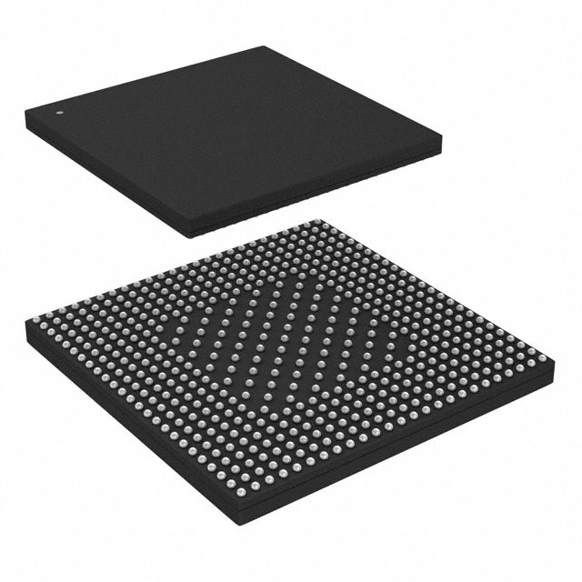
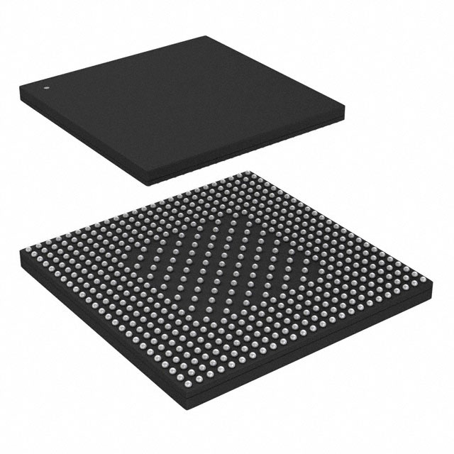
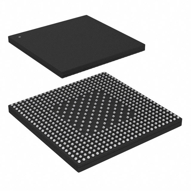
- Package & compliance – Surface-mount MAPBGA package (BGA 14×14 mm, 0.5 mm pitch) and RoHS compliant; industrial qualification.
Typical Applications
- Industrial control and automation – Low-power real-time control combined with application-level processing and secure boot makes it suitable for embedded controllers and factory automation nodes.
- User interfaces and HMIs – Graphics acceleration and MIPI-DSI support enable responsive displays and GUI-driven operator interfaces.
- Secure edge devices and gateways – Built-in Crypto/TRNG and secure boot provide hardware-backed security for connected industrial and IoT gateways.
- Sensor and data-acquisition modules – Multiple ADC channels, serial interfaces (UART/I2C/SPI) and low-power modes suit sensor hubs and distributed measurement units.
Unique Advantages
- Heterogeneous processing architecture: Combines a Cortex-A7 application domain with a Cortex-M4 real-time domain to separate rich OS workloads from deterministic control tasks.
- Flexible performance scaling: Multiple operating points including very-low-power run modes let designers trade performance and power to match application needs.
- Integrated security stack: Hardware crypto, TRNG, secure boot and programmable fuses help protect device identity and secure the boot chain.
- Broad peripheral set: Comprehensive I/O (USB 2.0, SD/MMC/eMMC, UART, I2C, SPI, FlexIO) and analog peripherals reduce external component count for compact designs.
- Compact industrial package: MAPBGA 14×14 mm package and surface-mount mounting provide a small footprint suitable for space-constrained boards.
Why Choose MCIMX7U3CVP06SD?
The MCIMX7U3CVP06SD delivers a pragmatic mix of application-class processing and low-power real-time control in a single, industrial-qualified device. Its integrated memory, multimedia, security and rich peripheral interfaces make it well-suited for designers building power-sensitive embedded systems, industrial HMIs, secure edge gateways and sensor hubs.
As part of the i.MX 7ULP family from NXP Semiconductors, this processor offers documented technical details and architecture continuity for designs that require scalability, integrated security and dependable long-term availability.
Request a quote today to get pricing and availability for the MCIMX7U3CVP06SD and to discuss how it fits your next embedded design.





















Date Founded: 2006
Headquarters: Eindhoven, North Brabant, Netherlands
Employees: 38,000+
Revenue: $10.53 Billion
Certifications and Memberships: ISO9001:2015, IATF16949:2016


