
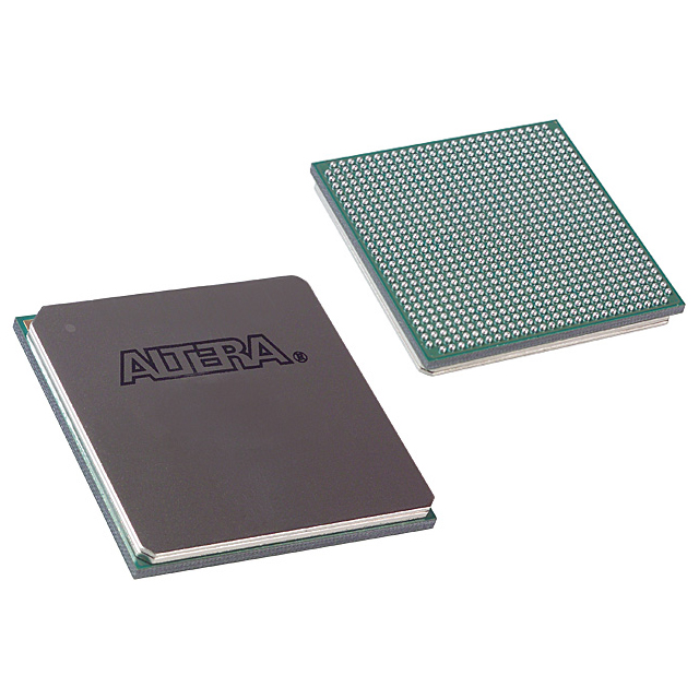
10AX016E3F27I1HG
| Part Description |
Arria 10 GX Field Programmable Gate Array (FPGA) IC 240 10086400 160000 672-BBGA, FCBGA |
|---|---|
| Quantity | 1,735 Available (as of June 15, 2026) |

| Product Category | Field Programmable Gate Array (FPGA) |
|---|---|
| Manufacturer | Intel |
| Manufacturing Status | Active |
| Manufacturer Standard Lead Time | 12 Weeks |
| Datasheet |
Specifications & Environmental
| Device Package | 672-FBGA (27x27) | Grade | Industrial | Operating Temperature | -40°C – 100°C | ||
|---|---|---|---|---|---|---|---|
| Package / Case | 672-BBGA, FCBGA | Number of I/O | 240 | Voltage | 870 mV - 980 mV | ||
| Mounting Method | Surface Mount | RoHS Compliance | RoHS Compliant | REACH Compliance | REACH Unaffected | ||
| Moisture Sensitivity Level | 3 (168 Hours) | Number of LABs/CLBs | 61510 | Number of Logic Elements/Cells | 160000 | ||
| Number of Gates | N/A | ECCN | 5A002A1 | HTS Code | 8542.39.0001 | ||
| Qualification | N/A | Total RAM Bits | 10086400 |
Overview of 10AX016E3F27I1HG – Arria 10 GX FPGA, 672-FBGA (27×27)
The 10AX016E3F27I1HG is an Intel Arria 10 GX field-programmable gate array (FPGA) supplied in a 672-FBGA (27×27) package. It is part of the Arria 10 family of 20 nm mid-range FPGAs and SoCs and is built for applications that require substantial logic, embedded memory, and flexible I/O in a surface-mount package.
Typical use cases include mid-range communications, compute acceleration, and broadcast or imaging systems where on-chip resources, industrial temperature operation, and power-optimized supply ranges are important design considerations.
Key Features
- Logic Capacity Provides 160,000 logic elements to implement complex custom logic and state machines.
- Embedded Memory Includes 10,086,400 total RAM bits of on-chip memory for buffering, packet processing, and data-path storage.
- I/O Resources Offers 240 user I/O pins suitable for interfaces and peripheral connectivity.
- Arria 10 Family Architecture Built on the Arria 10 device family architecture, which includes features such as adaptive logic modules, variable-precision DSP blocks, and embedded memory blocks as described in the device overview.
- Clocking and PLLs Arria 10 devices incorporate clock networks and PLL clock sources, including fractional synthesis and I/O PLLs, to support diverse clocking topologies.
- High-speed IP and Transceivers The family overview lists PCIe Gen1/Gen2/Gen3 hard IP and enhanced PCS hard IP for protocols such as Interlaken and 10 Gbps Ethernet, along with low-power serial transceivers and configurable PMA/PCS features.
- Package & Mounting 672-FBGA (27×27) package, designed for surface-mount assembly.
- Operating Conditions Industrial-grade operation with an operating temperature range of −40 °C to 100 °C and a supply voltage range of 870 mV to 980 mV.
- Compliance RoHS compliant.
Typical Applications
- Wireless Infrastructure Channel processing and backhaul applications that benefit from on-chip DSP resources and high logic density.
- Wireline & Networking Line cards, muxponders, and transponders using embedded memory and high-speed serial interfaces for packet aggregation and transport.
- Broadcast & Pro AV Studio switching, video transport, and professional audio/video processing leveraging large on-chip memory and logic capacity.
- Compute & Storage Acceleration Flash cache, cloud compute acceleration, and server offload tasks that use programmable logic and embedded memory.
- Medical & Imaging Diagnostic imaging and scanner systems that need deterministic processing and the industrial temperature range.
Unique Advantages
- High Logic Density: 160,000 logic elements enable complex, high-performance custom logic implementations without external ASICs.
- Significant On-Chip Memory: Over 10 million bits of embedded RAM reduce external memory dependence and simplify data-path designs.
- Flexible I/O in a Compact Package: 240 I/Os in a 672-FBGA (27×27) package provide a balance of connectivity and board-level footprint.
- Industrial Temperature Range: −40 °C to 100 °C operation supports deployment in demanding thermal environments.
- Power-Optimized Supply Window: Supported supply range of 870 mV to 980 mV facilitates power-aware design and supply planning.
- Arria 10 Family Capabilities: Family-level features such as DSP blocks, PLLs, transceivers, and PCIe hard IP provide integration options that accelerate system design.
Why Choose 10AX016E3F27I1HG?
The 10AX016E3F27I1HG delivers a robust combination of logic capacity, embedded memory, and I/O in a surface-mount 672-FBGA package suitable for industrial operation. Its placement within the Intel Arria 10 family provides a range of architectural features—DSP blocks, clocking resources, transceivers, and PCIe hard IP—that support mid-range communications, compute acceleration, and high-performance embedded applications.
Designers seeking a scalable, programmable platform with verifiable on-chip resources and industrial temperature support will find this Arria 10 GX device a practical choice for systems requiring significant on-chip RAM and logic while maintaining compact board-level integration.
Request a quote or submit an inquiry to receive pricing, availability, and lead-time information for 10AX016E3F27I1HG.


Date Founded: 1968
Headquarters: Santa Clara, California, USA
Employees: 130,000+
Revenue: $54.23 Billion
Certifications and Memberships: ISO9001:2015, ISO14001:2015, ISO17025:2017, ISO27001:2022, ISO45001:2018, ISO50001:2018


