
10AX027E3F27I2SG
| Part Description |
Arria 10 GX Field Programmable Gate Array (FPGA) IC 240 17870848 270000 672-BBGA, FCBGA |
|---|---|
| Quantity | 136 Available (as of June 15, 2026) |

| Product Category | Field Programmable Gate Array (FPGA) |
|---|---|
| Manufacturer | Intel |
| Manufacturing Status | Active |
| Manufacturer Standard Lead Time | 16 Weeks |
| Datasheet |
Specifications & Environmental
| Device Package | 672-FBGA, FC (27x27) | Grade | Industrial | Operating Temperature | -40°C – 100°C | ||
|---|---|---|---|---|---|---|---|
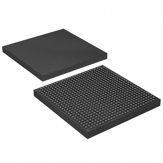
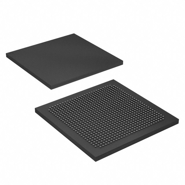
| Package / Case | 672-BBGA, FCBGA | Number of I/O | 240 | Voltage | 870 mV - 930 mV | ||
| Mounting Method | Surface Mount | RoHS Compliance | RoHS Compliant | REACH Compliance | REACH Unaffected | ||
| Moisture Sensitivity Level | 3 (168 Hours) | Number of LABs/CLBs | 101620 | Number of Logic Elements/Cells | 270000 | ||
| Number of Gates | N/A | ECCN | 5A002A1 | HTS Code | 8542.39.0001 | ||
| Qualification | N/A | Total RAM Bits | 17870848 |
Overview of 10AX027E3F27I2SG – Arria 10 GX FPGA, 270,000 logic elements, 240 I/O
The Intel Arria 10 GX 10AX027E3F27I2SG is a 20 nm mid-range, high-performance, power-efficient field programmable gate array (FPGA) IC. It combines a large logic fabric with substantial on-chip memory and flexible I/O to address midrange applications that need performance and power efficiency.
Typical use cases for this device include wireless and wireline infrastructure, broadcast and video equipment, computing and storage acceleration, medical imaging, and defense systems where processing density, embedded memory capacity, and industrial operating range are required.
Key Features
- Core Logic — 270,000 logic elements provide a high-density programmable fabric for complex digital functions and custom processing pipelines.
- On-chip Memory — 17,870,848 total RAM bits of embedded memory support large buffering, packet processing, and cache-like functions on-chip.
- I/O and Interfaces — 240 user I/O pins enable wide parallel interfaces and multiple serial/transceiver connections suitable for diverse system topologies.
- Family-level IP and Blocks — Arria 10 family features include adaptive logic modules, variable-precision DSP blocks, embedded memory blocks, PLL clock networks, PCIe Gen1/2/3 hard IP, and low-power serial transceivers, enabling common system functions to be implemented efficiently.
- Power Supply — Core voltage supply range of 870 mV to 930 mV supports the device’s optimized power architecture.
- Package and Mounting — Supplied in a 672-ball BGA FCBGA (27 × 27 mm) package for high-density board integration; surface-mount mounting type.
- Industrial Temperature Grade — Rated for operation from −40 °C to 100 °C for deployment in industrial environments.
- Compliance — RoHS compliant.
Typical Applications
- Wireless Infrastructure: Channel and switch cards in remote radio heads and mobile backhaul equipment where programmable processing and power efficiency are critical.
- Wireline Networking: 40G/100G muxponders, transponders, and line cards for bridging and aggregation that require high-speed interfaces and packet buffering.
- Broadcast and Pro AV: Studio switching, video transport, and videoconferencing systems that leverage on-chip memory and programmable logic for format conversion and real-time processing.
- Computing and Storage: Flash cache, server acceleration, and cloud computing nodes that need hardware acceleration and flexible logic partitioning.
- Imaging and Defense: Diagnostic imaging systems and radar/electronic warfare applications that require dense DSP, embedded memory, and robust operating temperature range.
Unique Advantages
- High logic density: 270,000 logic elements enable consolidation of complex logic and accelerator functions into a single device, reducing system BOM and board area.
- Substantial on-chip memory: Nearly 18 Mb of embedded RAM supports large buffers and on-chip data paths, minimizing external memory bandwidth needs.
- Broad family IP support: Arria 10 family features such as variable-precision DSP blocks, PLLs, and PCIe hard IP simplify implementation of common interfaces and signal processing tasks.
- Industrial-ready temperature range: −40 °C to 100 °C rating supports deployment in a wide range of environmental conditions without additional thermal qualification steps.
- Compact, high-density package: 672-ball FCBGA (27 × 27 mm) delivers high pin count and signal density for complex board-level designs.
- Controlled core power envelope: Core supply range (870–930 mV) aligns with low-voltage power domains used in modern FPGA power architectures.
Why Choose 10AX027E3F27I2SG?
The 10AX027E3F27I2SG positions itself as a versatile mid-range FPGA that balances performance and power efficiency, leveraging the Arria 10 family’s architecture and IP building blocks. With 270,000 logic elements, substantial embedded RAM, and 240 I/O, it is well suited to system designs that demand significant on-chip resources for packet processing, DSP acceleration, and flexible I/O integration.
This device is appropriate for engineers and system designers building midrange networking, broadcast, computing, or industrial systems that require programmable hardware density, family-level IP options, and an industrial operating range. Its combination of logic capacity, memory, and package density supports scalable designs and long-term deployment.
Request a quote or submit an inquiry to get pricing, lead time, and availability for the 10AX027E3F27I2SG Arria 10 GX FPGA.


Date Founded: 1968
Headquarters: Santa Clara, California, USA
Employees: 130,000+
Revenue: $54.23 Billion
Certifications and Memberships: ISO9001:2015, ISO14001:2015, ISO17025:2017, ISO27001:2022, ISO45001:2018, ISO50001:2018


