
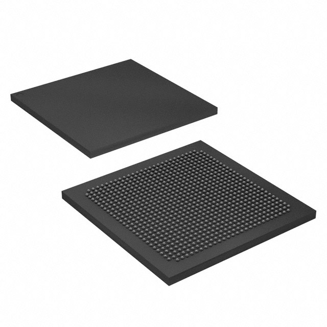
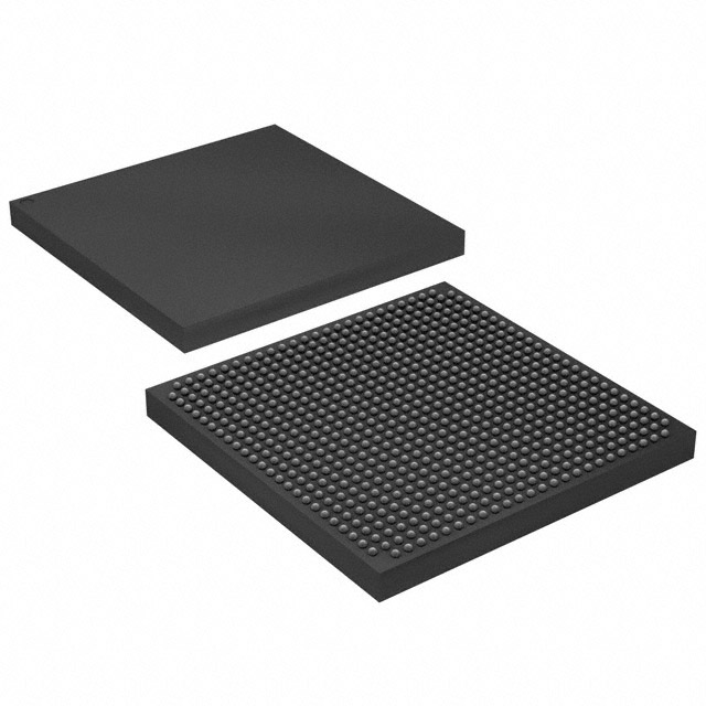
10AX027E3F29E2LG
| Part Description |
Arria 10 GX Field Programmable Gate Array (FPGA) IC 360 17870848 270000 780-BBGA, FCBGA |
|---|---|
| Quantity | 235 Available (as of June 15, 2026) |

| Product Category | Field Programmable Gate Array (FPGA) |
|---|---|
| Manufacturer | Intel |
| Manufacturing Status | Active |
| Manufacturer Standard Lead Time | 12 Weeks |
| Datasheet |
Specifications & Environmental
| Device Package | 780-FBGA, FC (29x29) | Grade | Extended | Operating Temperature | 0°C – 100°C | ||
|---|---|---|---|---|---|---|---|
| Package / Case | 780-BBGA, FCBGA | Number of I/O | 360 | Voltage | 870 mV - 930 mV | ||
| Mounting Method | Surface Mount | RoHS Compliance | RoHS Compliant | REACH Compliance | REACH Unaffected | ||
| Moisture Sensitivity Level | 3 (168 Hours) | Number of LABs/CLBs | 101620 | Number of Logic Elements/Cells | 270000 | ||
| Number of Gates | N/A | ECCN | 5A002A1 | HTS Code | 8542.39.0001 | ||
| Qualification | N/A | Total RAM Bits | 17870848 |
Overview of 10AX027E3F29E2LG – Arria 10 GX FPGA, 270,000 Logic Elements, 780‑BBGA
The 10AX027E3F29E2LG is an Intel Arria 10 GX field programmable gate array (FPGA) in a 780‑ball FCBGA package. It is part of the Arria 10 family of 20‑nm mid‑range FPGAs designed for applications that require a balance of performance and power efficiency.
This device targets mid‑range systems across wireless, wireline, broadcast, computing and storage, medical, and military markets, delivering programmable logic capacity, embedded memory, and high‑speed I/O in a compact surface‑mount package.
Key Features
- Programmable Logic Capacity 270,000 logic elements for complex programmable logic and control functions.
- Logic Structure 101,620 adaptive logic modules (ALMs) reported in family documentation to support fine‑grained logic and arithmetic implementations.
- On‑Chip Memory 17,870,848 total RAM bits to support buffer, cache, and temporary storage needs inside the FPGA fabric.
- I/O 360 I/O pins to interface with external peripherals, memory, and high‑speed interfaces.
- High‑Speed Interfaces and IP Device family features include PCIe Gen1/Gen2/Gen3 hard IP, enhanced PCS hard IP for Interlaken and 10 Gbps Ethernet, and low‑power serial transceivers as documented in the family overview.
- DSP and Clocking Family documentation cites variable‑precision DSP blocks, clock networks, PLLs, and fractional synthesis capabilities for datapath and timing design.
- Package 780‑BBGA (FCBGA), supplier package listed as 780‑FBGA, FC (29×29), surface‑mount for board‑level integration.
- Power Nominal voltage supply range 870 mV to 930 mV for core power domains.
- Operating Range and Grade Extended grade with an operating temperature range of 0 °C to 100 °C.
- Compliance RoHS compliant.
Typical Applications
- Wireless Infrastructure Channel and switch cards for remote radio heads and mobile backhaul systems where programmable logic and transceiver capability are required.
- Wireline Networking 40G/100G muxponders, transponders, and line cards benefiting from embedded memory and high‑speed interface IP.
- Broadcast and Pro AV Studio switching, video transport, and professional audio/video processing using on‑chip memory and DSP resources.
- Computing and Storage Server acceleration and flash cache applications that leverage programmable logic capacity and integrated interfaces.
- Medical and Defense Systems Diagnostic imaging, radar, and secure communications where mid‑range FPGA performance and flexibility are needed.
Unique Advantages
- High Logic Density: 270,000 logic elements provide ample programmable fabric for complex control, signal processing, and protocol handling.
- Substantial On‑Chip Memory: Nearly 18 Mbits of RAM bits reduce external memory dependence for buffering and temporary data storage.
- Integrated High‑Speed I/O and IP: Family features such as PCIe hard IP and enhanced PCS support simplify implementation of high‑bandwidth links.
- Power‑Aware Design: Documented family emphasis on power efficiency and a defined core supply range (870–930 mV) support optimized power delivery and thermal planning.
- Compact Surface‑Mount Package: 780‑ball FCBGA (29×29) enables dense board integration while providing a large I/O count.
- Documented Ecosystem: The Arria 10 device family is supported by detailed device handbooks and device‑level documentation to assist design and validation.
Why Choose 10AX027E3F29E2LG?
The 10AX027E3F29E2LG combines substantial programmable logic, embedded memory, and a wide complement of I/O in a surface‑mount 780‑ball FCBGA package, making it a practical choice for mid‑range systems that require both performance and power efficiency. Its Extended grade thermal range and RoHS compliance make it suitable for a variety of commercial and mission‑critical applications documented for the Arria 10 family.
Designs that need a balance of logic density, on‑chip RAM, and integrated high‑speed interface IP will benefit from this device, backed by Arria 10 family documentation and technical references for development and deployment.
Request a quote or submit an inquiry to receive pricing, lead time, and availability information for the 10AX027E3F29E2LG.


Date Founded: 1968
Headquarters: Santa Clara, California, USA
Employees: 130,000+
Revenue: $54.23 Billion
Certifications and Memberships: ISO9001:2015, ISO14001:2015, ISO17025:2017, ISO27001:2022, ISO45001:2018, ISO50001:2018


