
10AX032E1F29I1SG
| Part Description |
Arria 10 GX Field Programmable Gate Array (FPGA) IC 360 21040128 320000 780-BBGA, FCBGA |
|---|---|
| Quantity | 520 Available (as of June 15, 2026) |

| Product Category | Field Programmable Gate Array (FPGA) |
|---|---|
| Manufacturer | Intel |
| Manufacturing Status | Discontinued |
| Manufacturer Standard Lead Time | 13 Weeks |
| Datasheet |
Specifications & Environmental
| Device Package | 780-FBGA (29x29) | Grade | Industrial | Operating Temperature | -40°C – 100°C | ||
|---|---|---|---|---|---|---|---|
| Package / Case | 780-BBGA, FCBGA | Number of I/O | 360 | Voltage | 870 mV - 980 mV | ||
| Mounting Method | Surface Mount | RoHS Compliance | RoHS Compliant | REACH Compliance | REACH Unaffected | ||
| Moisture Sensitivity Level | 3 (168 Hours) | Number of LABs/CLBs | 119900 | Number of Logic Elements/Cells | 320000 | ||
| Number of Gates | N/A | ECCN | 5A002A1 | HTS Code | 8542.39.0001 | ||
| Qualification | N/A | Total RAM Bits | 21040128 |
Overview of 10AX032E1F29I1SG – Arria 10 GX Field Programmable Gate Array (FPGA), 320,000 logic elements
The 10AX032E1F29I1SG is an Intel Arria 10 GX Field Programmable Gate Array delivered in a 780-BBGA FCBGA package. It is part of the Arria 10 family of 20 nm mid-range FPGAs and SoCs, designed for applications that require a balance of high logic capacity and power efficiency.
With a combination of 320,000 logic elements, 21,040,128 total RAM bits and 360 I/O, this device targets mid-range designs across wireless, wireline, broadcast, computing/storage, medical and defense markets where performance, integration and industrial operating range are important.
Key Features
- Logic Capacity — 320,000 logic elements to implement complex custom logic, control functions and datapaths.
- Embedded Memory — 21,040,128 total RAM bits for on-chip buffering, packet processing or algorithmic state storage.
- I/O Density — 360 I/O pins to connect multiple external interfaces, memory devices or front-end peripherals.
- Arria 10 Architecture — Part of the Intel Arria 10 20 nm family, offering architecture-level features such as embedded memory blocks, variable-precision DSP blocks, PLLs and low-power serial transceivers as described in the device family documentation.
- Power Supply — Core supply range 0.870 V to 0.980 V, enabling designs that match the device’s specified voltage window.
- Industrial Temperature Range — Rated for operation from −40 °C to 100 °C for deployment in temperature-challenging environments.
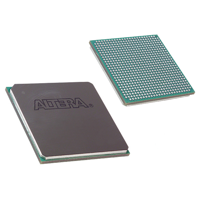
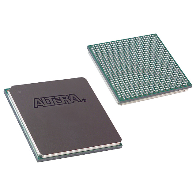
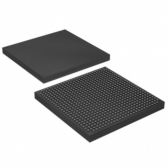
- Package & Mounting — 780-BBGA (FCBGA) package, supplier device package 780-FBGA (29×29), surface-mount mounting type for high-density PCB assembly.
- Compliance — RoHS compliant.
Typical Applications
- Wireless Infrastructure — Channel and switch cards in remote radio heads and mobile backhaul equipment that require programmable logic and high I/O density.
- Wireline & Optical Networking — Line cards, muxponders and transponders where on-chip memory and FPGA logic handle packet aggregation and protocol bridging.
- Broadcast & Professional AV — Studio switches and video transport systems that need real-time processing and deterministic I/O.
- Compute & Storage Acceleration — Cloud servers and flash-cache acceleration tasks that utilize embedded memory and programmable datapaths.
- Imaging & Medical Equipment — Diagnostic scanners and imaging systems that benefit from programmable logic, embedded RAM and industrial temperature operation.
Unique Advantages
- High logical density: 320,000 logic elements let you integrate large custom logic blocks and algorithmic functions on a single device, reducing external component count.
- Substantial on-chip RAM: 21,040,128 bits of embedded memory provide significant local buffering and state storage for data-path and signal-processing tasks.
- Robust I/O capability: 360 I/O pins enable complex system-level interfacing without requiring extensive external glue logic.
- Industrial readiness: −40 °C to 100 °C operating range supports deployment in harsh or temperature-variable environments.
- Compact, production-ready package: 780-BBGA FCBGA (780-FBGA, 29×29) surface-mount package allows high-density board integration and reliable assembly.
- Part of a documented device family: Backed by Intel Arria 10 device documentation that details architecture features such as DSP blocks, PLLs, transceivers and configuration options.
Why Choose 10AX032E1F29I1SG?
The 10AX032E1F29I1SG positions itself as a capable mid-range Arria 10 GX FPGA that brings together a large logic resource, significant embedded RAM and extensive I/O in a production-focused FCBGA package. Its industrial temperature rating and RoHS compliance make it suitable for designs that require durability and regulatory conformity.
Engineers targeting wireless infrastructure, networking, broadcast, compute acceleration or imaging systems will find the device’s balance of integration and family-level features—documented in Arria 10 resources—useful for reducing BOM complexity and accelerating development.
Request a quote or submit an inquiry for pricing and availability of the 10AX032E1F29I1SG to begin integrating this Arria 10 GX FPGA into your next design.


Date Founded: 1968
Headquarters: Santa Clara, California, USA
Employees: 130,000+
Revenue: $54.23 Billion
Certifications and Memberships: ISO9001:2015, ISO14001:2015, ISO17025:2017, ISO27001:2022, ISO45001:2018, ISO50001:2018


