
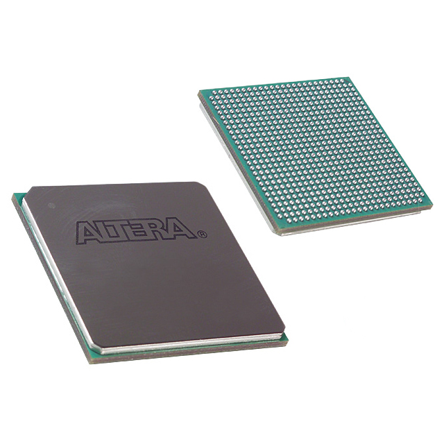
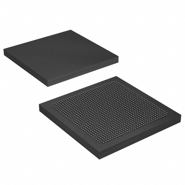
10AX032E1F27I1SG
| Part Description |
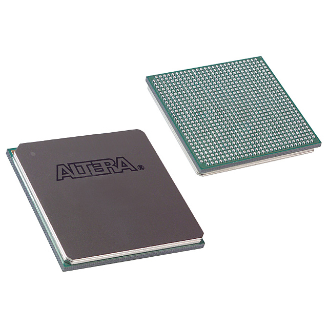
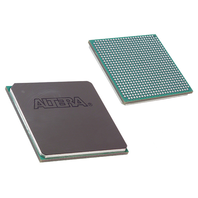
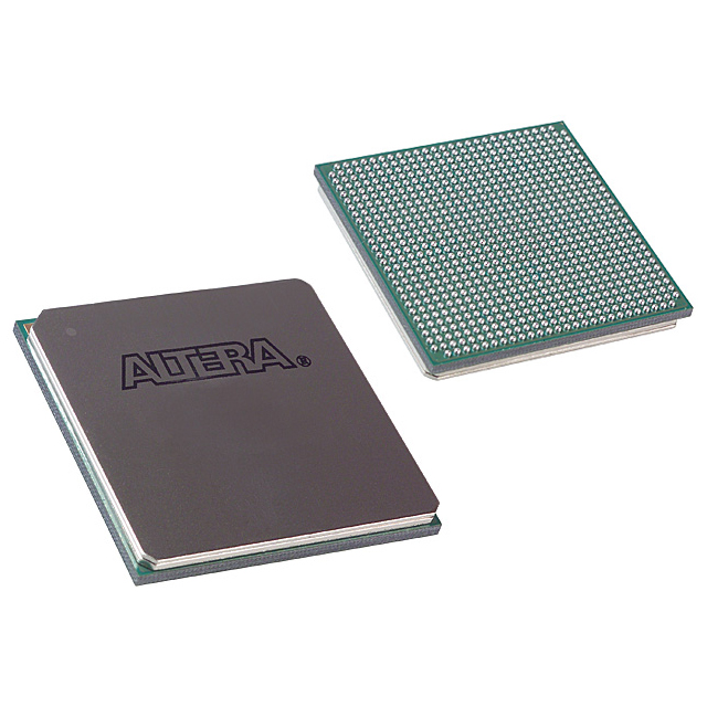
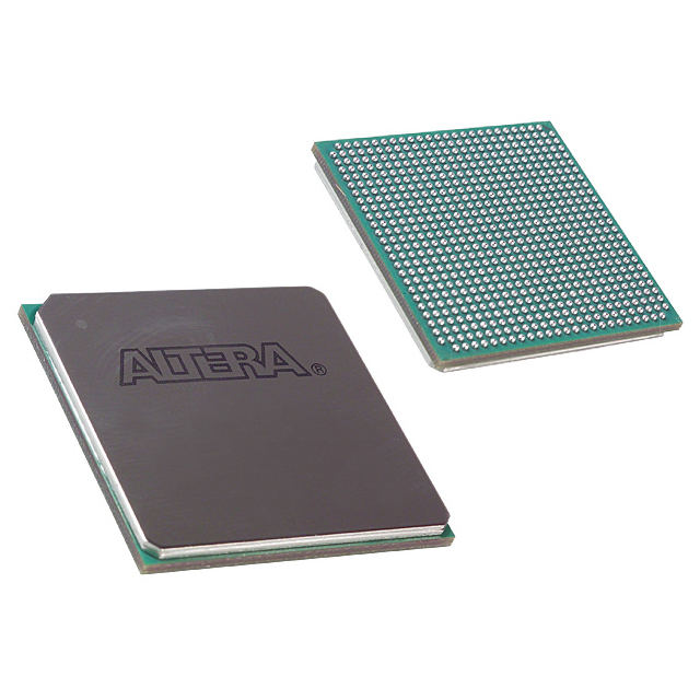
Arria 10 GX Field Programmable Gate Array (FPGA) IC 240 21040128 320000 672-BBGA, FCBGA |
|---|---|
| Quantity | 532 Available (as of October 8, 2026) |
| Product Category | Field Programmable Gate Array (FPGA) |
|---|---|
| Manufacturer | Intel |
| Manufacturing Status | Discontinued |
| Manufacturer Standard Lead Time | 13 Weeks |
| Datasheet |
Specifications & Environmental
| Device Package | 672-FBGA (27x27) | Grade | Industrial | Operating Temperature | -40°C – 100°C | ||
|---|---|---|---|---|---|---|---|
| Package / Case | 672-BBGA, FCBGA | Number of I/O | 240 | Voltage | 870 mV - 980 mV | ||
| Mounting Method | Surface Mount | RoHS Compliance | RoHS Compliant | REACH Compliance | REACH Unaffected | ||
| Moisture Sensitivity Level | 3 (168 Hours) | Number of LABs/CLBs | 119900 | Number of Logic Elements/Cells | 320000 | ||
| Number of Gates | N/A | ECCN | 5A002A1 | HTS Code | 8542.39.0001 | ||
| Qualification | N/A | Total RAM Bits | 21040128 |
Overview of 10AX032E1F27I1SG – Arria 10 GX FPGA, 320000 logic elements, 21,040,128 RAM bits
The 10AX032E1F27I1SG is an Intel Arria 10 GX field-programmable gate array (FPGA) in a 672-ball BGA package, targeted at mid-range, high-performance applications. Built on the Arria 10 device family architecture, it combines a large logic fabric with substantial embedded RAM and a broad I/O complement to support data‑intensive, power‑sensitive designs.
Typical markets and use cases include wireless and wireline communications, broadcast and video processing, computing and storage acceleration, medical imaging, and defense systems where performance, integration, and industrial temperature operation are required.
Key Features
- Logic Capacity 320,000 logic elements (cells) to implement complex custom logic, control, and data-path functions.
- Embedded Memory 21,040,128 total RAM bits of on-chip memory for buffering, lookup tables, and state storage.
- I/O Resources 240 user I/Os to interface with external peripherals, memory devices, and high-speed interfaces.
- Device Family Architecture Arria 10 family features including adaptive logic modules, variable‑precision DSP blocks, embedded memory blocks, and advanced clock networks for system-level integration and performance scaling.
- Hard IP and Transceivers Family-level support for PCIe Gen1/Gen2/Gen3 hard IP and high-speed serial transceiver features to simplify protocol implementation and external connectivity.
- Power and Supply Core voltage supply range of 870 mV to 980 mV, reflecting the device's mid-range power architecture and support for power-optimization techniques.
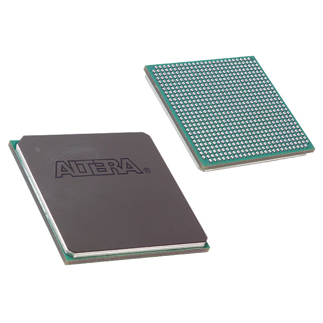
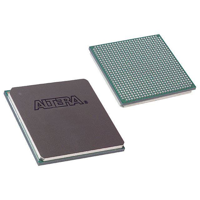
- Package & Mounting 672-BBGA (FCBGA) package with supplier device package listed as 672-FBGA (27×27); surface-mount mounting type for standard PCB assembly processes.
- Temperature & Grade Industrial grade operation with an operating temperature range of −40 °C to 100 °C for deployment in temperature‑challenging environments.
- Compliance RoHS‑compliant to meet environmental and regulatory requirements.
Typical Applications
- Wireless Infrastructure Channel and switch cards in remote radio heads and mobile backhaul functions that require flexible DSP and high I/O counts.
- Wireline & Optical Networking 40G/100G muxponders, transponders and line cards where embedded memory and hard IP accelerate packet processing and protocol handling.
- Broadcast & Professional AV Studio switches, video transport and conferencing systems leveraging large logic capacity and on‑chip RAM for real‑time video processing.
- Compute & Storage Acceleration Server acceleration and flash cache applications that use FPGA logic and memory to offload compute‑intensive tasks.
- Medical & Defense Systems Diagnostic imaging, radar, and electronic warfare systems that benefit from high logic density, deterministic I/O, and industrial temperature operation.
Unique Advantages
- High logic density: 320,000 logic elements enable large-scale custom logic and complex system integration on a single device, reducing external component count.
- Substantial on‑chip memory: 21,040,128 RAM bits support deep buffering, lookup tables, and state machines without immediate reliance on external memory.
- Broad I/O coverage: 240 user I/Os provide flexible interfacing options for peripherals, memory interfaces, and multi-protocol designs.
- Industrial temperature rating: −40 °C to 100 °C operation supports deployment in temperature-challenging industrial and field environments.
- System-ready package: 672-ball BGA (27×27) surface-mount package allows dense PCB routing and standard assembly processes for volume production.
- RoHS compliant: Conforms to environmental requirements for lead‑free manufacturing and end-product compliance.
Why Choose 10AX032E1F27I1SG?
The 10AX032E1F27I1SG positions itself as a mid-range, high-performance FPGA option within the Intel Arria 10 family, offering a balance of large logic resources, significant embedded memory, and extensive I/O in a production-ready industrial package. Its architectural features—adaptive logic modules, DSP blocks, clock networks, and family-level hard IP—support complex data-paths and protocol acceleration while enabling power-optimized designs through the device family's power-saving technologies.
This part is suited for engineering teams building communications, video, compute-acceleration, medical imaging, or defense systems that require on-chip capacity, rugged temperature operation, and a compact BGA footprint. The combination of logic, memory, and I/O simplifies board-level design and helps shorten time to market while supporting scalable design requirements.
Request a quote or submit a parts inquiry to check availability and pricing for 10AX032E1F27I1SG. Our team can provide lead-time information and support your component selection and procurement process.





















Date Founded: 1968
Headquarters: Santa Clara, California, USA
Employees: 130,000+
Revenue: $54.23 Billion
Certifications and Memberships: ISO9001:2015, ISO14001:2015, ISO17025:2017, ISO27001:2022, ISO45001:2018, ISO50001:2018


