
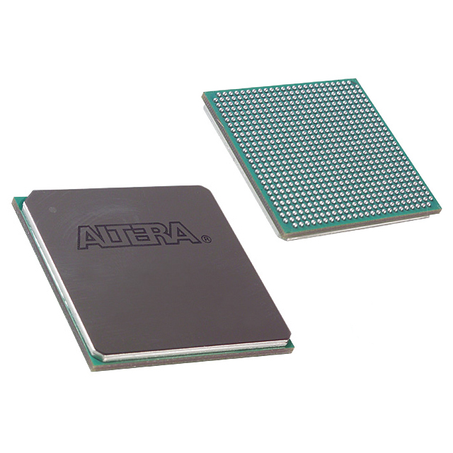
10AX032E1F27I1HG
| Part Description |
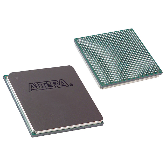
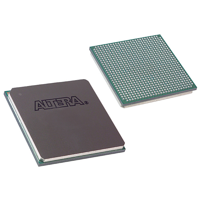
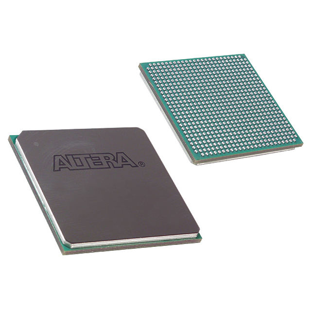
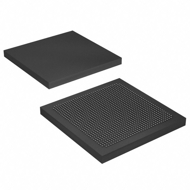
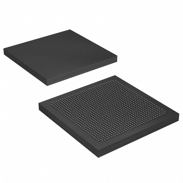
Arria 10 GX Field Programmable Gate Array (FPGA) IC 240 21040128 320000 672-BBGA, FCBGA |
|---|---|
| Quantity | 222 Available (as of October 7, 2026) |
| Product Category | Field Programmable Gate Array (FPGA) |
|---|---|
| Manufacturer | Intel |
| Manufacturing Status | Active |
| Manufacturer Standard Lead Time | 16 Weeks |
| Datasheet |
Specifications & Environmental
| Device Package | 672-FBGA (27x27) | Grade | Industrial | Operating Temperature | -40°C – 100°C | ||
|---|---|---|---|---|---|---|---|
| Package / Case | 672-BBGA, FCBGA | Number of I/O | 240 | Voltage | 870 mV - 980 mV | ||
| Mounting Method | Surface Mount | RoHS Compliance | RoHS Compliant | REACH Compliance | REACH Unaffected | ||
| Moisture Sensitivity Level | 3 (168 Hours) | Number of LABs/CLBs | 119900 | Number of Logic Elements/Cells | 320000 | ||
| Number of Gates | N/A | ECCN | 5A002A1 | HTS Code | 8542.39.0001 | ||
| Qualification | N/A | Total RAM Bits | 21040128 |
Overview of 10AX032E1F27I1HG – Arria 10 GX FPGA, 320,000 logic elements, 672-FBGA
The 10AX032E1F27I1HG is an Intel Arria 10 GX field programmable gate array (FPGA) in a 672-ball FBGA package intended for mid-range, performance-sensitive designs. It combines a 20 nm architecture with substantial programmable logic, embedded memory, and high-density I/O to address applications across wireless, wireline, broadcast, computing, medical, and defense markets.
Key on-package specifications include 320,000 logic elements, 21,040,128 total RAM bits, 240 general-purpose I/O pins, industrial-grade operation, and a supply range of 870 mV to 980 mV—features that support high-integration board designs and industrial operating environments.
Key Features
- 20 nm Device Family Arria 10 devices are described as 20 nm mid-range FPGAs and SoCs offering higher performance and improved power efficiency compared with prior mid-range generations.
- Logic Capacity 320,000 logic elements provide substantial programmable resources for complex mid-range designs.
- Embedded Memory 21,040,128 total RAM bits of on-chip memory to support buffering, caching, and on-chip data structures.
- I/O and Package 240 I/O pins in a 672-BBGA (672-FBGA, 27×27) package for dense board-level integration and routing flexibility.
- Power and Thermal Supply voltage range from 870 mV to 980 mV; rated operating temperature range from −40 °C to 100 °C for industrial deployment.
- Mounting and Compliance Surface-mount package and RoHS compliance for standard PCB assembly and environmental compliance.
- Built-in IP and Reconfiguration Device overview references integrated IP and capabilities such as PCIe Gen1/2/3 hard IP, enhanced PCS hard IP for Interlaken and 10 Gbps Ethernet, low-power serial transceivers, and support for dynamic and partial reconfiguration.
Typical Applications
- Wireless infrastructure Channel cards, switch cards, and mobile backhaul systems can leverage the logic density and transceiver features for protocol processing and high-speed interfaces.
- Wireline networking Line cards, muxponders, and transponders (including 40G/100G use cases) benefit from high logic and embedded memory capacity for packet processing and aggregation.
- Broadcast and AV systems Studio switches, conferencing, and professional audio/video equipment can use the device for routing, format conversion, and timing-critical processing.
- Computing and storage Server acceleration, flash cache, and cloud infrastructure modules can exploit on-chip memory and reconfiguration features for acceleration and caching tasks.
- Medical and defense systems Diagnostic imaging, radar, electronic warfare, and secure communications where industrial temperature operation and reconfigurable logic are required.
Unique Advantages
- High logic and memory density: 320,000 logic elements and over 21 million RAM bits enable complex mid-range designs without external logic proliferation.
- Power-efficient 20 nm architecture: Device family positioning emphasizes improved power efficiency for performance-sensitive applications.
- Industrial operating range: Rated from −40 °C to 100 °C, supporting deployments in demanding environmental conditions.
- Dense I/O and package options: 240 I/O in a 672-FBGA (27×27) footprint for compact, high-density board layouts.
- Integrated protocol and reconfiguration support: On-device hard IP for PCIe and high-speed Ethernet, plus support for dynamic and partial reconfiguration to adapt designs in the field.
- Assembly and regulatory readiness: Surface-mount packaging and RoHS compliance simplify manufacturing and environmental compliance.
Why Choose 10AX032E1F27I1HG?
The 10AX032E1F27I1HG positions itself as a high-capacity, industrial-grade Arria 10 GX FPGA suited for mid-range applications that require a balance of logic density, embedded memory, and protocol IP. Its 20 nm architecture and integrated feature set support designs that need in-field reconfiguration, high-speed interfaces, and robust thermal operation.
This part is appropriate for engineering teams building network infrastructure, compute acceleration modules, broadcast systems, and industrial devices where on-chip memory, substantial logic resources, and reliable operation across −40 °C to 100 °C are critical considerations.
Request a quote or submit an inquiry to receive pricing, availability, and technical support information for the 10AX032E1F27I1HG.




















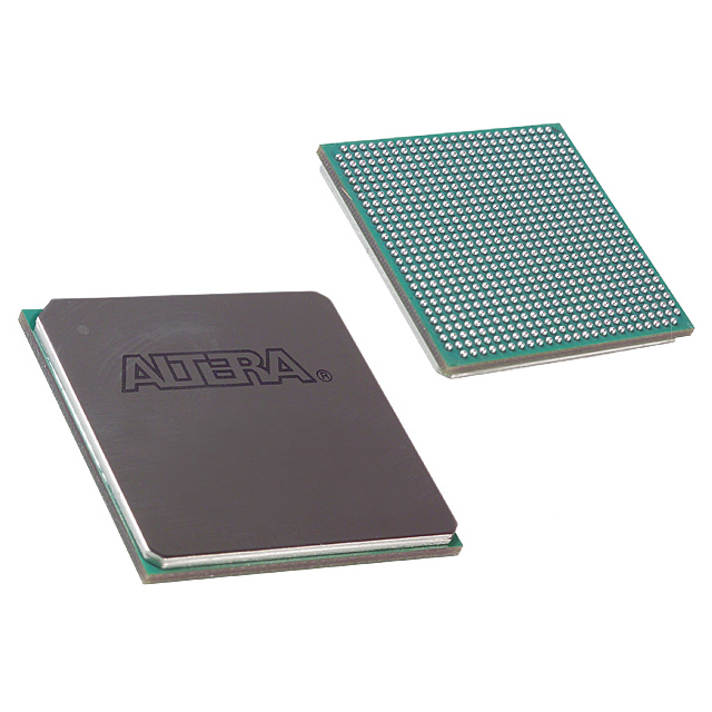
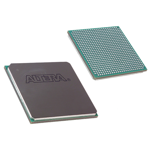
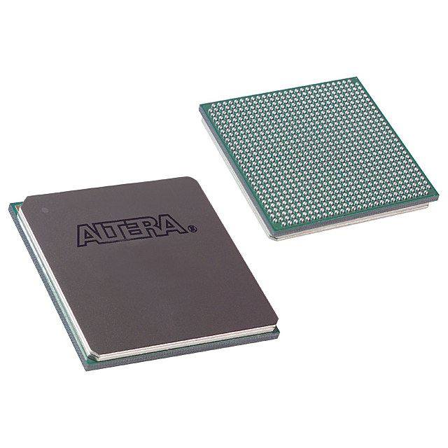

Date Founded: 1968
Headquarters: Santa Clara, California, USA
Employees: 130,000+
Revenue: $54.23 Billion
Certifications and Memberships: ISO9001:2015, ISO14001:2015, ISO17025:2017, ISO27001:2022, ISO45001:2018, ISO50001:2018


