
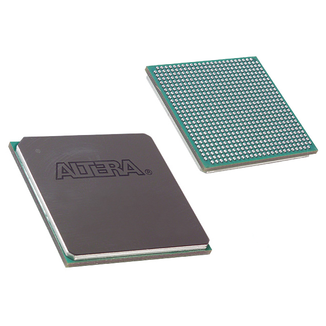
10AX027H4F35I3LG
| Part Description |
Arria 10 GX Field Programmable Gate Array (FPGA) IC 384 17870848 270000 1152-BBGA, FCBGA |
|---|---|
| Quantity | 645 Available (as of June 15, 2026) |

| Product Category | Field Programmable Gate Array (FPGA) |
|---|---|
| Manufacturer | Intel |
| Manufacturing Status | Active |
| Manufacturer Standard Lead Time | 16 Weeks |
| Datasheet |
Specifications & Environmental
| Device Package | 1152-FBGA, FC (35x35) | Grade | Industrial | Operating Temperature | -40°C – 100°C | ||
|---|---|---|---|---|---|---|---|
| Package / Case | 1152-BBGA, FCBGA | Number of I/O | 384 | Voltage | 870 mV - 980 mV | ||
| Mounting Method | Surface Mount | RoHS Compliance | RoHS Compliant | REACH Compliance | REACH Unaffected | ||
| Moisture Sensitivity Level | 3 (168 Hours) | Number of LABs/CLBs | 101620 | Number of Logic Elements/Cells | 270000 | ||
| Number of Gates | N/A | ECCN | 5A002A1 | HTS Code | 8542.39.0001 | ||
| Qualification | N/A | Total RAM Bits | 17870848 |
Overview of 10AX027H4F35I3LG – Arria 10 GX FPGA, 1152‑BBGA (Industrial)
The 10AX027H4F35I3LG is an Intel Arria 10 GX field‑programmable gate array (FPGA) IC in a 1152‑BBGA FCBGA package designed for mid‑range, high‑performance applications. Built on a 20 nm architecture, this device delivers a combination of high logic density, substantial embedded memory, and a broad set of I/O and system features suited to communication, compute, and video systems.
With 270,000 logic elements, 17,870,848 total RAM bits and 384 I/O pins, the device targets market segments such as wireless, wireline, broadcast, computing and storage, and other applications requiring balanced performance and power efficiency. The part is specified for industrial operation and supports low‑voltage core operation for power‑sensitive designs.
Key Features
- Core Logic 270,000 logic elements provide substantial programmable logic capacity for mid‑range FPGA designs.
- Embedded Memory 17,870,848 total RAM bits for on‑chip data buffering, packet processing, and memory‑intensive functions.
- I/O and Interfaces 384 I/O pins support diverse external interfaces and board integration requirements.
- Transceivers and High‑Speed I/O Family features include low‑power serial transceivers and enhanced PCS hard IP for Interlaken and 10 Gbps Ethernet (as described for Arria 10 devices).
- System IP and Connectivity Available hard IP in the device family includes PCIe Gen1/Gen2/Gen3 and other communication-centric blocks to simplify system integration.
- Clocking and PLLs Comprehensive clock networks and PLL clock sources, including fractional synthesis and I/O PLLs, support complex timing and clocking topologies.
- Power Core voltage supply range of 0.870 V to 0.980 V enables low‑voltage operation and supports power‑sensitive designs.
- Package and Mounting 1152‑BBGA (FCBGA) supplier package (1152‑FBGA, FC 35×35) in a surface‑mount form factor for compact board implementation.
- Temperature and Grade Industrial‑grade operation from −40 °C to 100 °C for deployment in temperature‑challenging environments.
- Compliance RoHS compliant.
Typical Applications
- Wireless infrastructure — Channel and switch cards in remote radio heads and mobile backhaul systems leveraging the device's logic density and transceiver features.
- Wireline networking — 40G/100G muxponders, transponders, and line cards using the device family's high‑speed serial and PCS hard IP capabilities.
- Compute and storage — Server acceleration, flash cache, and cloud computing functions that benefit from large embedded memory and programmable logic resources.
- Broadcast and professional AV — Studio switches, videoconferencing, and professional audio/video processing where on‑chip memory and I/O flexibility aid system integration.
Unique Advantages
- High programmable capacity: 270,000 logic elements allow complex custom logic implementations without external ASICs.
- Substantial on‑chip memory: Nearly 18 Mbits of embedded RAM enables local buffering, frame storage, and efficient data handling.
- Rich I/O and high‑speed connectivity: 384 I/Os plus family support for serial transceivers and PCIe hard IP streamline interface design and reduce external components.
- Industrial‑grade thermal range: Specified for −40 °C to 100 °C operation to meet rugged application requirements.
- Low‑voltage core operation: 0.870–0.980 V supply range supports lower power envelopes in energy‑sensitive systems.
- Compact system‑level package: 1152‑BBGA FCBGA package reduces PCB footprint while providing dense routing for high‑pin‑count designs.
Why Choose 10AX027H4F35I3LG?
The 10AX027H4F35I3LG Arria 10 GX FPGA combines a high logic element count and substantial embedded memory with family features such as advanced clocking, hard IP for high‑speed interfaces, and low‑power transceivers. This balance of programmable capacity, on‑chip memory, and interface options makes it well suited for mid‑range systems in communications, compute, and professional AV markets where performance and power efficiency are both important.
Designed for industrial environments and supplied in a compact 1152‑BBGA package, the device supports designs that require robust thermal range, dense integration, and reduced BOM complexity. Its feature set aligns with projects demanding scalable logic, integrated system IP, and a path to deployable, production‑ready FPGA-based solutions.
Request a quote or submit an inquiry to receive pricing and availability for 10AX027H4F35I3LG and to discuss how this Arria 10 GX device fits your next design.


Date Founded: 1968
Headquarters: Santa Clara, California, USA
Employees: 130,000+
Revenue: $54.23 Billion
Certifications and Memberships: ISO9001:2015, ISO14001:2015, ISO17025:2017, ISO27001:2022, ISO45001:2018, ISO50001:2018


